As of late 2025, the global semiconductor industry is standing at the precipice of a historic milestone. Analysts from McKinsey, Gartner, and PwC are now in consensus: the global semiconductor market is on a definitive trajectory to reach $1 trillion in annual revenue by 2030. This represents a staggering doubling of the industry’s size within a single decade, a feat driven not by traditional consumer electronics cycles, but by a structural shift in the global economy. At the heart of this expansion is the pervasive integration of artificial intelligence, a booming automotive silicon sector, and the massive expansion of the digital infrastructure required to power the next generation of computing.
The transition from a $500 billion industry to a $1 trillion powerhouse marks a "Semiconductor Decade" where silicon has become the most critical commodity on earth. This growth is being fueled by an unprecedented "silicon squeeze," as the demand for high-performance compute, specialized AI accelerators, and power-efficient chips for electric vehicles outstrips the capacity of even the most advanced fabrication plants. With capital expenditure for new fabs expected to top $1 trillion through 2030, the industry is effectively rebuilding the foundation of modern civilization on a bed of advanced microprocessors.
Technical Evolution: From Transistors to Token Generators
The technical engine behind this $1 trillion march is the evolution of AI from simple generative models to "Physical AI" and "Agentic AI." In 2025, the industry has moved beyond the initial excitement of text-based Large Language Models (LLMs) into an era of independent reasoning agents and autonomous robotics. These advancements require a fundamental shift in chip architecture. Unlike traditional CPUs designed for general-purpose tasks, the new generation of AI silicon—led by architectures like NVIDIA’s (NASDAQ: NVDA) Blackwell and its successors—is optimized for massive parallel processing and high-speed "token generation." This has led to a surge in demand for High Bandwidth Memory (HBM) and advanced packaging techniques like Chip-on-Wafer-on-Substrate (CoWoS), which allow multiple chips to be integrated into a single high-performance package.
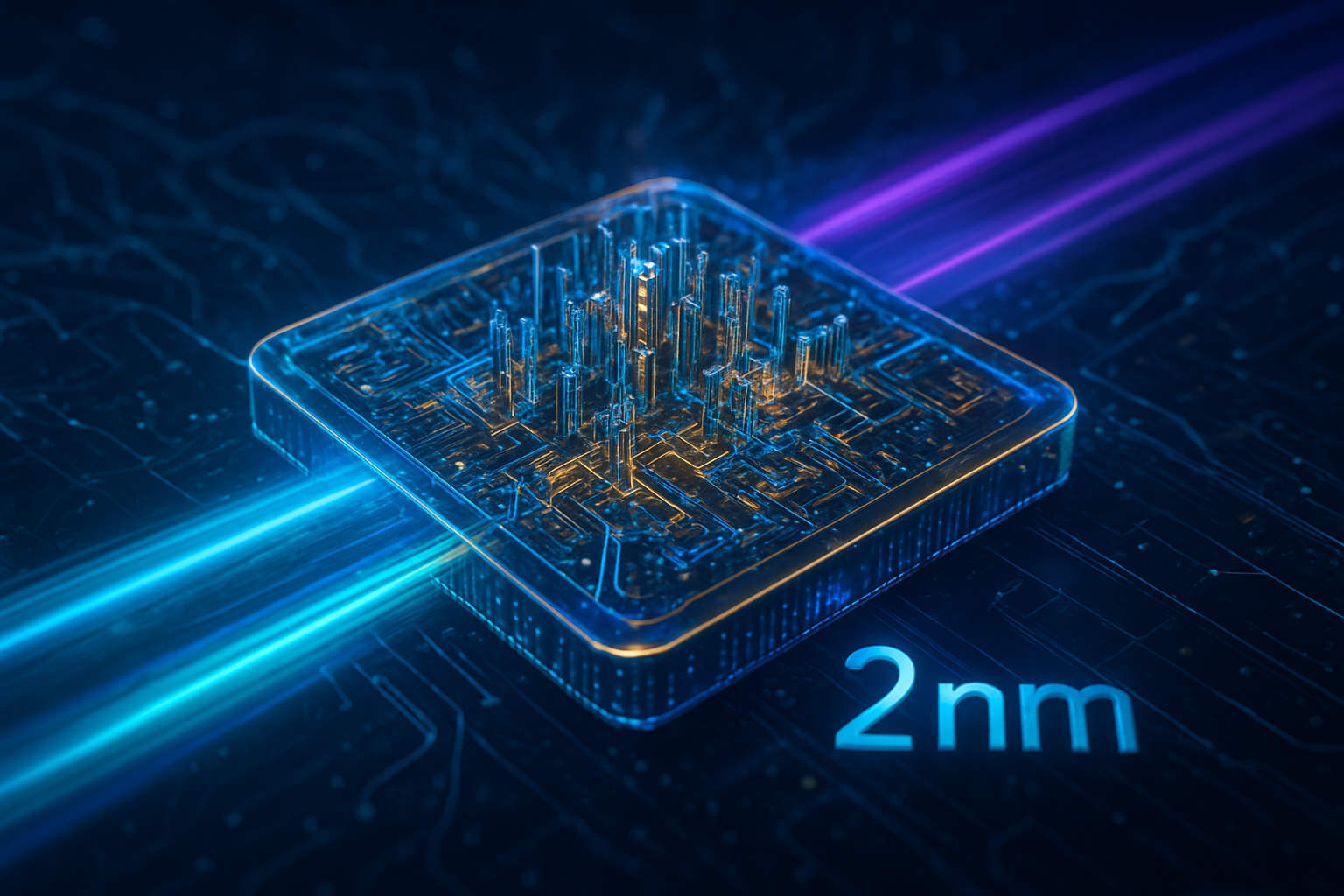
Technically, the industry is pushing the boundaries of physics as it moves toward 2nm and 1.4nm process nodes. Foundries like TSMC (NYSE: TSM) are utilizing High-NA (Numerical Aperture) Extreme Ultraviolet (EUV) lithography from ASML (NASDAQ: ASML) to print features at a scale once thought impossible. Furthermore, the rise of the "Software-Defined Vehicle" (SDV) has introduced a new technical frontier: power electronics. The shift to Electric Vehicles (EVs) has necessitated the use of wide-bandgap materials like Silicon Carbide (SiC) and Gallium Nitride (GaN), which can handle higher voltages and temperatures more efficiently than traditional silicon. An average EV now contains over $1,500 worth of semiconductor content, nearly triple that of a traditional internal combustion engine vehicle.
Industry experts note that this era differs from the previous "mobile era" because of the sheer density of value in each wafer. While smartphones moved billions of units, AI chips represent a massive increase in silicon value density. A single AI accelerator can cost tens of thousands of dollars, reflecting the immense research and development and manufacturing complexity involved. The AI research community has reacted with a mix of awe and urgency, noting that the "compute moat"—the ability for well-funded labs to access massive clusters of these chips—is becoming the primary differentiator in the race toward Artificial General Intelligence (AGI).
Market Dominance and the Competitive Landscape
The march toward $1 trillion has cemented the dominance of a few key players while creating massive opportunities for specialized startups. NVIDIA (NASDAQ: NVDA) remains the undisputed titan of the AI era, with a market capitalization that has soared past $4 trillion as it maintains a near-monopoly on high-end AI training hardware. However, the landscape is diversifying. Broadcom (NASDAQ: AVGO) has emerged as a critical linchpin in the AI ecosystem, providing the networking silicon and custom Application-Specific Integrated Circuits (ASICs) that allow hyperscalers like Google and Meta to build their own proprietary AI hardware.
Memory manufacturers have also seen a dramatic reversal of fortune. SK Hynix (KRX: 000660) and Micron (NASDAQ: MU) have seen their revenues double as the demand for HBM4 and HBM4E memory—essential for feeding data to hungry AI GPUs—reaches fever pitch. Samsung (KRX: 005930), while facing stiff competition in the logic space, remains a formidable Integrated Device Manufacturer (IDM) that benefits from the rising tide of both memory and foundry demand. For traditional giants like Intel (NASDAQ: INTC) and AMD (NASDAQ: AMD), the challenge has been to pivot their roadmaps toward "AI PCs" and data center accelerators to keep pace with the shifting market dynamics.
Strategic advantages are no longer just about design; they are about "sovereign AI" and supply chain security. Nations are increasingly treating semiconductor manufacturing as a matter of national security, leading to a fragmented but highly subsidized global market. Startups specializing in "Edge AI"—chips designed to run AI locally on devices rather than in the cloud—are finding new niches in the industrial and medical sectors. This shift is disrupting existing products, as "dumb" sensors and controllers are replaced by intelligent silicon capable of real-time computer vision and predictive maintenance.
The Global Significance of the Silicon Surge
The projection of a $1 trillion market is more than just a financial milestone; it represents the total "siliconization" of the global economy. This trend fits into the broader AI landscape as the physical manifestation of the digital intelligence boom. Just as the 19th century was defined by steel and the 20th by oil, the 21st century is being defined by the semiconductor. This has profound implications for global power dynamics, as the "Silicon Shield" of Taiwan and the technological rivalry between the U.S. and China dictate diplomatic and economic strategies.
However, this growth comes with significant concerns. The environmental impact of massive new fabrication plants and the energy consumption of AI data centers are under intense scrutiny. The industry is also facing a critical talent shortage, with an estimated gap of one million skilled workers by 2030. Comparisons to previous milestones, such as the rise of the internet or the smartphone, suggest that while the growth is real, it may lead to periods of extreme volatility and overcapacity if the expected AI utility does not materialize as quickly as the hardware is built.
Despite these risks, the consensus remains that the "compute-driven" economy is here to stay. The integration of AI into every facet of life—from healthcare diagnostics to autonomous logistics—requires a foundation of silicon that simply did not exist five years ago. This milestone is a testament to the industry's ability to innovate under pressure, overcoming the end of Moore’s Law through advanced packaging and new materials.
Future Horizons: Toward 2030 and Beyond
Looking ahead, the next five years will be defined by the transition to "Physical AI." We expect to see the first wave of truly capable humanoid robots and autonomous transport systems hitting the mass market, each requiring a suite of sensors and inference chips that will drive the next leg of semiconductor growth. Near-term developments will likely focus on the rollout of 2nm production and the integration of optical interconnects directly onto chip packages to solve the "memory wall" and "power wall" bottlenecks that currently limit AI performance.
Challenges remain, particularly in the realm of geopolitics and material supply. The industry must navigate trade restrictions on critical materials like gallium and germanium while building out regional supply chains. Experts predict that the next phase of the market will see a shift from "general-purpose AI" to "vertical AI," where chips are custom-designed for specific industries such as genomics, climate modeling, or high-frequency finance. This "bespoke silicon" era will likely lead to even higher margins for design firms and foundries.
The long-term vision is one where compute becomes a ubiquitous utility, much like electricity. As we approach the 2030 milestone, the focus will likely shift from building the infrastructure to optimizing it for efficiency and sustainability. The "Road to $1 Trillion" is not just a destination but a transformation of how humanity processes information and interacts with the physical world.
A New Era of Computing
The semiconductor industry's journey to a $1 trillion valuation is a landmark event in technological history. It signifies the end of the "Information Age" and the beginning of the "Intelligence Age," where the ability to generate and apply AI is the primary driver of economic value. The key takeaway for investors and industry observers is that the current growth is structural, not cyclical; the world is being re-platformed onto AI-native hardware.
As we move through 2026 and toward 2030, the most critical factors to watch will be the resolution of the talent gap, the stability of the global supply chain, and the actual deployment of "Agentic AI" in enterprise environments. The $1 trillion mark is a symbol of the industry's success, but the true impact will be measured by the breakthroughs in science, medicine, and productivity that this massive compute power enables. The semiconductor market has doubled in size, but its influence on the future of humanity has grown exponentially.
This content is intended for informational purposes only and represents analysis of current AI developments.
TokenRing AI delivers enterprise-grade solutions for multi-agent AI workflow orchestration, AI-powered development tools, and seamless remote collaboration platforms.
For more information, visit https://www.tokenring.ai/.