Tag: TSMC

  • The Memory Margin Flip: Samsung and SK Hynix Set to Surpass TSMC Margins Amid HBM3e Explosion

    The Memory Margin Flip: Samsung and SK Hynix Set to Surpass TSMC Margins Amid HBM3e Explosion

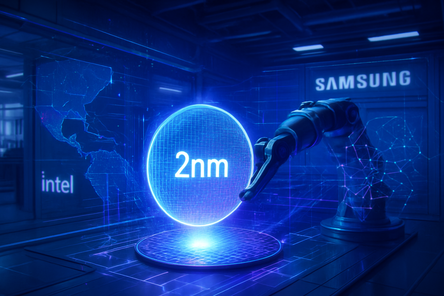
    In a historic shift for the semiconductor industry, the long-standing hierarchy of profitability is being upended. For years, the pure-play foundry model pioneered by Taiwan Semiconductor Manufacturing Company (NYSE: TSM) has been the gold standard for financial performance, consistently delivering gross margins that left memory makers in the dust. However, as of late 2025, a "margin flip" is underway. Driven by the insatiable demand for High-Bandwidth Memory (HBM3e) and the looming transition to HBM4, South Korean giants Samsung (KRX: 005930) and SK Hynix (KRX: 000660) are now projected to surpass TSMC in gross margins, marking a pivotal moment in the AI hardware era.

    This seismic shift is fueled by a perfect storm of supply constraints and the technical evolution of AI clusters. As the industry moves from training massive models to the high-volume inference stage, the "memory wall"—the bottleneck created by the speed at which data can be moved from memory to the processor—has become the primary constraint for tech giants. Consequently, memory is no longer a cyclical commodity; it has become the most precious real estate in the AI data center, allowing memory manufacturers to command unprecedented pricing power and record-breaking profits.

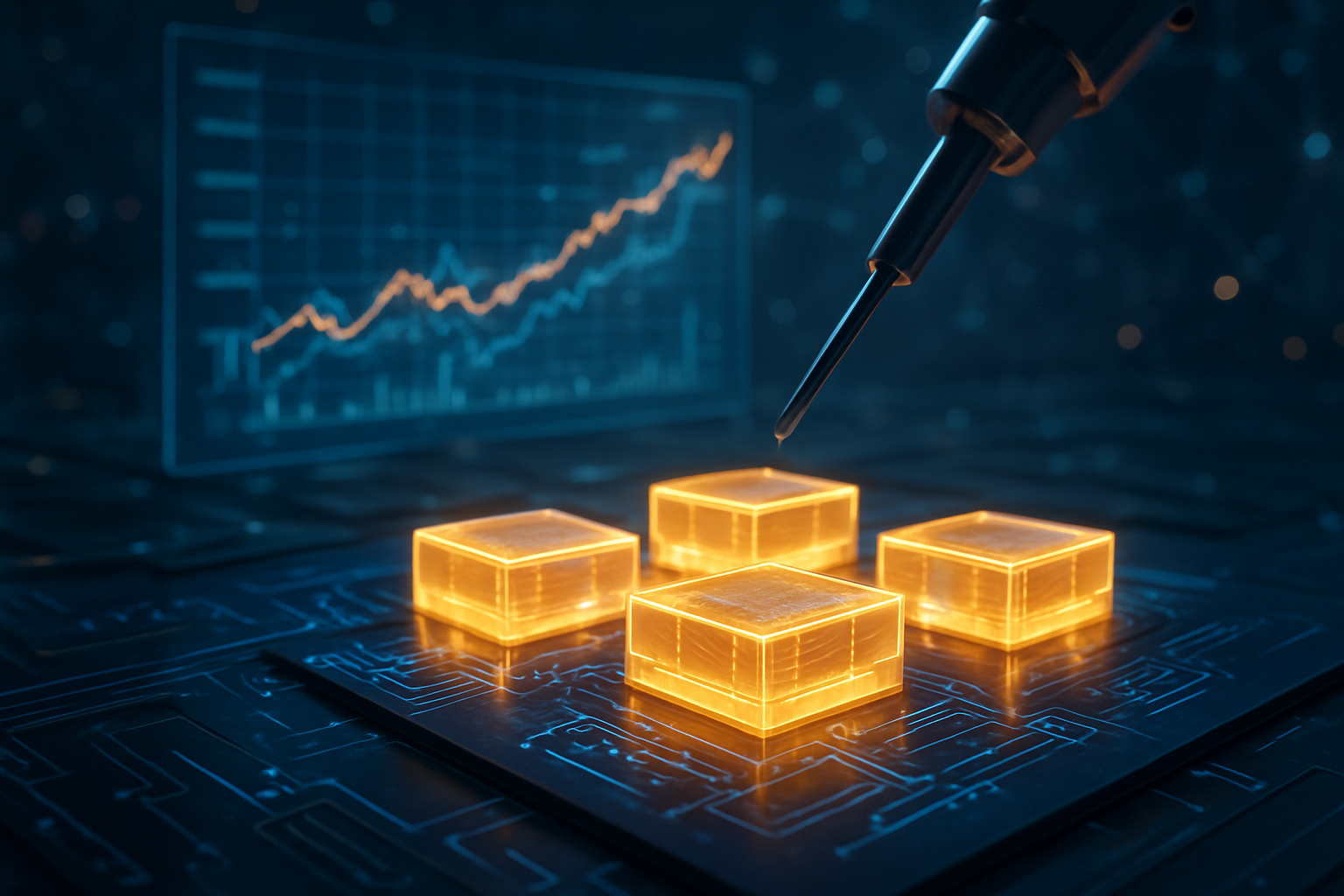
    The Technical Engine: HBM3e and the Death of the Memory Wall

    The technical specifications of HBM3e represent a quantum leap over its predecessors, specifically designed to meet the demands of trillion-parameter Large Language Models (LLMs). While standard HBM3 offered bandwidths of roughly 819 GB/s, the HBM3e stacks currently shipping in late 2025 have shattered the 1.2 TB/s barrier. This 50% increase in bandwidth, coupled with pin speeds exceeding 9.2 Gbps, allows AI accelerators to feed data to logic units at rates previously thought impossible. Furthermore, the transition to 12-high (12-Hi) stacking has pushed capacity to 36GB per cube, enabling systems like NVIDIA’s latest Blackwell-Ultra architecture to house nearly 300GB of high-speed memory on a single package.

    This technical dominance is reflected in the projected gross margins for Q4 2025. Analysts now forecast that Samsung’s memory division and SK Hynix will see gross margins ranging between 63% and 67%, while TSMC is expected to maintain a stable but lower range of 59% to 61%. The disparity stems from the fact that while TSMC must grapple with the massive capital expenditures of its 2nm transition and the dilution from new overseas fabs in Arizona and Japan, the memory makers are benefiting from a global shortage that has allowed them to hike server DRAM prices by over 60% in a single year.

    Initial reactions from the AI research community highlight that the focus has shifted from raw FLOPS (floating-point operations per second) to "effective throughput." Experts note that in late 2025, the performance of an AI cluster is more closely correlated with its HBM capacity and bandwidth than the clock speed of its GPUs. This has effectively turned Samsung and SK Hynix into the new gatekeepers of AI performance, a role traditionally held by the logic foundries.

    Strategic Maneuvers: NVIDIA and AMD in the Crosshairs

    For major chip designers like NVIDIA (NASDAQ: NVDA) and AMD (NASDAQ: AMD), this shift has necessitated a radical change in supply chain strategy. NVIDIA, in particular, has moved to a "strategic capacity capture" model. To ensure it isn't sidelined by the HBM shortage, NVIDIA has entered into massive prepayment agreements, with purchase obligations reportedly reaching $45.8 billion by mid-2025. These prepayments effectively finance the expansion of SK Hynix and Micron (NASDAQ: MU) production lines, ensuring that NVIDIA remains first in line for the most advanced HBM3e and HBM4 modules.

    AMD has taken a different approach, focusing on "raw density" to challenge NVIDIA’s dominance. By integrating 288GB of HBM3e into its MI325X series, AMD is betting that hyperscalers like Meta (NASDAQ: META) and Google (NASDAQ: GOOGL) will prefer chips that can run massive models on fewer nodes, thereby reducing the total cost of ownership. This strategy, however, makes AMD even more dependent on the yields and pricing of the memory giants, further empowering Samsung and SK Hynix in price negotiations.

    The competitive landscape is also seeing the rise of alternative memory solutions. To mitigate the extreme costs of HBM, NVIDIA has begun utilizing LPDDR5X—typically found in high-end smartphones—for its Grace CPUs. This allows the company to tap into high-volume consumer supply chains, though it remains a stopgap for the high-performance requirements of the H100 and Blackwell successors. The move underscores a growing desperation among logic designers to find any way to bypass the high-margin toll booths set up by the memory makers.

    The Broader AI Landscape: Supercycle or Bubble?

    The "Memory Margin Flip" is more than just a corporate financial milestone; it represents a structural shift in the value of the semiconductor stack. Historically, memory was treated as a low-margin, high-volume commodity. In the AI era, it has become "specialized logic," with HBM4 introducing custom base dies that allow memory to be tailored to specific AI workloads. This evolution fits into the broader trend of "vertical integration" where the distinction between memory and computing is blurring, as seen in the development of Processing-in-Memory (PIM) technologies.

    However, this rapid ascent has sparked concerns of an "AI memory bubble." Critics argue that the current 60%+ margins are unsustainable and driven by "double-ordering" from hyperscalers like Amazon (NASDAQ: AMZN) who are terrified of being left behind. If AI adoption plateaus or if inference techniques like 4-bit quantization significantly reduce the need for high-bandwidth data access, the industry could face a massive oversupply crisis by 2027. The billions being poured into "Mega Fabs" by SK Hynix and Samsung could lead to a glut that crashes prices just as quickly as they rose.

    Comparatively, proponents of the "Supercycle" theory argue that this is the "early internet" phase of accelerated computing. They point out that unlike the dot-com bubble, the 2025 boom is backed by the massive cash flows of the world’s most profitable companies. The shift from general-purpose CPUs to accelerated GPUs and TPUs is a permanent architectural change in global infrastructure, meaning the demand for data bandwidth will remain insatiable for the foreseeable future.

    Future Horizons: HBM4 and Beyond

    Looking ahead to 2026, the transition to HBM4 will likely cement the memory makers' dominance. HBM4 is expected to carry a 40% to 50% price premium over HBM3e, with unit prices projected to reach the mid-$500 range. A key development to watch is the "custom base die," where memory makers may actually utilize TSMC’s logic processes for the bottom layer of the HBM stack. While this increases production complexity, it allows for even tighter integration with AI processors, further increasing the value-add of the memory component.

    Beyond HBM, we are seeing the emergence of new form factors like Socamm2—removable, stackable modules being developed by Samsung in partnership with NVIDIA. These modules aim to bring HBM-like performance to edge-AI and high-end workstations, potentially opening up a massive new market for high-margin memory outside of the data center. The challenge remains the extreme precision required for manufacturing; even a minor drop in yield for these 12-high and 16-high stacks can erase the profit gains from high pricing.

    Conclusion: A New Era of Semiconductor Power

    The projected margin flip of late 2025 marks the end of an era where logic was king and memory was an afterthought. Samsung and SK Hynix have successfully navigated the transition from commodity suppliers to indispensable AI partners, leveraging the physical limitations of data movement to capture a larger share of the AI gold rush. As their gross margins eclipse those of TSMC, the power dynamics of the semiconductor industry have been fundamentally reset.

    In the coming months, the industry will be watching for the first official Q4 2025 earnings reports to see if these projections hold. The key indicators will be HBM4 sampling success and the stability of server DRAM pricing. If the current trajectory continues, the "Memory Margin Flip" will be remembered as the moment when the industry realized that in the age of AI, it doesn't matter how fast you can think if you can't remember the data.


    This content is intended for informational purposes only and represents analysis of current AI developments.

    TokenRing AI delivers enterprise-grade solutions for multi-agent AI workflow orchestration, AI-powered development tools, and seamless remote collaboration platforms.
    For more information, visit https://www.tokenring.ai/.

  • TSMC’s ‘N-2’ Geopolitical Hurdle: A Win for Samsung and Intel in the US?

    TSMC’s ‘N-2’ Geopolitical Hurdle: A Win for Samsung and Intel in the US?

    As of late 2025, the global race for semiconductor supremacy has hit a regulatory wall that is reshaping the American tech landscape. Taiwan’s strictly enforced "N-2" rule, a policy designed to keep the most advanced chip-making technology within its own borders, has created a significant technological lag for Taiwan Semiconductor Manufacturing Co. (NYSE: TSM) at its flagship Arizona facilities. While TSMC remains the world's leading foundry, this mandatory two-generation delay is opening a massive strategic window for its primary rivals to seize the "Made in America" market for next-generation AI silicon.

    The implications of this policy are becoming clear as we head into 2026: for the first time in decades, the most advanced chips produced on U.S. soil may not come from TSMC, but from Intel (NASDAQ: INTC) and Samsung Electronics (KRX: 005930). As domestic demand for 2nm-class production skyrockets—driven by the insatiable needs of AI and high-performance computing—the "N-2" rule is forcing top-tier American firms to reconsider their long-standing reliance on the Taiwanese giant.

    The N-2 Bottleneck: A Three-Year Lag in the Desert

    The "N-2" rule is a protective regulatory framework enforced by Taiwan’s Ministry of Economic Affairs and the National Science and Technology Council. It mandates that any semiconductor manufacturing technology deployed in TSMC’s overseas facilities must be at least two generations behind the leading-edge nodes currently in mass production in Taiwan. With TSMC having successfully ramped its 2nm (N2) process in Hsinchu and Kaohsiung in late 2025, the N-2 rule dictates that its Arizona "Fab 21" can legally produce nothing more advanced than 4nm or 5nm chips until the next major breakthrough occurs at home.

    This creates a stark disparity in technical specifications. While TSMC’s Taiwan fabs are currently churning out 2nm chips with refined Gate-All-Around (GAA) transistors for Apple (NASDAQ: AAPL) and Nvidia (NASDAQ: NVDA), the Arizona plant is restricted to older FinFET architectures. Industry experts note that this represents a roughly three-year technology gap. For U.S. customers requiring the power efficiency and transistor density of the 2nm node to remain competitive in the AI era, the "N-2" rule makes TSMC’s domestic U.S. offerings effectively obsolete for flagship products.

    The reaction from the semiconductor research community has been one of cautious pragmatism. While analysts acknowledge that the N-2 rule is essential for Taiwan’s "Silicon Shield"—the idea that its global indispensability prevents geopolitical aggression—it creates a "two-tier" supply chain. Experts at the Center for Strategic and International Studies (CSIS) have pointed out that this policy directly conflicts with the goals of the U.S. CHIPS Act, which sought to bring the most advanced manufacturing back to American shores, not just the "trailing edge" of the leading edge.

    Samsung and Intel: The New Domestic Leaders?

    Capitalizing on TSMC’s regulatory handcuffs, Intel and Samsung are moving aggressively to fill the 2nm vacuum in the United States. Intel is currently in the midst of its "five nodes in four years" sprint, with its 18A (1.8nm-class) process entering risk production in Arizona. Unlike TSMC, Intel is not bound by Taiwanese export controls, allowing it to deploy its most advanced innovations—such as PowerVia backside power delivery—directly in its U.S. fabs by early 2026. This technical advantage could allow Intel to leapfrog TSMC in the U.S. market for the first time in a decade.

    Samsung is following a similar trajectory with its massive $17 billion investment in Taylor, Texas. The South Korean firm is targeting mass production of 2nm (SF2) chips at the Taylor facility by the first half of 2026. Samsung’s strategic advantage lies in its mature GAA (Gate-All-Around) architecture, which it has been refining since its 3nm rollout. By offering a "turnkey" solution that includes advanced packaging and domestic 2nm production, Samsung is positioning itself as the primary alternative for companies that cannot wait for TSMC’s 2028 Arizona 2nm timeline.

    The shift in market positioning is already visible in the customer pipeline. AMD (NASDAQ: AMD) is reportedly pursuing a "dual-foundry" strategy, engaging in deep negotiations with Samsung to utilize the Taylor plant for its next-generation EPYC "Venice" server CPUs. Similarly, Google (NASDAQ: GOOGL) has dispatched teams to audit Samsung’s Texas operations for its future Tensor Processing Units (TPUs). For these tech giants, the priority has shifted from "who is the best overall" to "who can provide 2nm capacity within the U.S. today," and currently, the answer is not TSMC.

    Geopolitical Sovereignty vs. Supply Chain Reality

    The "N-2" rule highlights the growing tension between national security and globalized tech manufacturing. For Taiwan, the rule is a survival mechanism. By ensuring that the world’s most advanced AI chips can only be made in Taiwan, the island maintains its status as a critical node in the global economy that the West must protect. However, as the U.S. pushes for "AI Sovereignty"—the ability to design and manufacture the engines of AI entirely within domestic borders—Taiwan’s restrictions are beginning to look like a strategic liability for American firms.

    This development marks a departure from previous AI milestones. In the past, the software was the primary bottleneck; today, the physical location and generation of the silicon have become the defining constraints. The potential concern for the industry is a fragmentation of the AI hardware market. If Nvidia continues to rely on TSMC’s Taiwan-only 2nm production while AMD and Google pivot to Samsung’s U.S.-based 2nm, we may see a divergence in hardware capabilities based purely on geographic and regulatory factors rather than engineering prowess.

    Comparisons are being drawn to the early days of the Cold War's technology export controls, but with a modern twist. In this scenario, the "ally" (Taiwan) is the one restricting the "protector" (the U.S.) to maintain its own leverage. This dynamic is forcing a rapid maturation of the U.S. semiconductor ecosystem, as the CHIPS Act funding is increasingly diverted toward firms like Intel and Samsung who are willing to bypass the "N-2" logic and bring the bleeding edge to American soil immediately.

    The Road to 1.4nm and Beyond

    Looking ahead, the battle for the 2nm crown is just the opening act. TSMC has already announced its A14 (1.4nm) and A16 nodes, targeted for 2027 and 2028 in Taiwan. Under the current N-2 framework, this means the U.S. will not see 1.4nm production from TSMC until at least 2030. This persistent lag provides a multi-year window for Intel and Samsung to establish themselves as the "foundries of choice" for the U.S. defense and AI sectors, which are increasingly mandated to use domestic silicon.

    Future developments will likely focus on "Advanced Packaging" as a way to mitigate the N-2 rule's impact. TSMC may attempt to ship 2nm "chiplets" from Taiwan to be packaged in the U.S., but even this faces regulatory scrutiny. Meanwhile, experts predict that the U.S. government may increase pressure on the Taiwanese administration to move to an "N-1" or even "N-0" policy for specific "trusted" facilities in Arizona, though such a change would face stiff political opposition in Taipei.

    The primary challenge remains yield and reliability. While Intel and Samsung have the right to build 2nm in the U.S., they must still prove they can match TSMC’s legendary manufacturing consistency. If Samsung’s Taylor fab or Intel’s 18A process suffers from low yields, the "N-2" hurdle may matter less, as companies will still be forced to wait for TSMC’s superior, albeit distant, production.

    Summary: A New Map for the AI Era

    The "N-2" rule has fundamentally altered the trajectory of the American semiconductor industry. By mandating a technology lag for TSMC’s U.S. operations, Taiwan has inadvertently handed a golden opportunity to Intel and Samsung to capture the most lucrative segment of the domestic market. As AMD, Google, and Tesla (NASDAQ: TSLA) look to secure their AI futures, the geographic origin of their chips is becoming as important as the architecture itself.

    This development is a significant milestone in AI history, representing the moment when geopolitics officially became a primary architectural constraint for computer science. The next few months will be critical as Samsung’s Taylor plant begins equipment move-in and Intel’s 18A enters the final stages of validation. For the tech industry, the message is clear: the "Silicon Shield" is holding firm in Taiwan, but in the United States, the race for 2nm is wide open.


    This content is intended for informational purposes only and represents analysis of current AI developments.

    TokenRing AI delivers enterprise-grade solutions for multi-agent AI workflow orchestration, AI-powered development tools, and seamless remote collaboration platforms.
    For more information, visit https://www.tokenring.ai/.

  • Strategic Silence: Why TSMC’s Arizona Grand Opening Delay Signals a New Era of Semiconductor Diplomacy

    Strategic Silence: Why TSMC’s Arizona Grand Opening Delay Signals a New Era of Semiconductor Diplomacy

    The semiconductor industry stood at a standstill in late 2024 when Taiwan Semiconductor Manufacturing Company (NYSE:TSM) made the calculated decision to postpone the grand opening ceremony of its landmark Fab 21 in Phoenix, Arizona. Originally rumored for December 2024, the event was pushed into early 2025, a move that many industry insiders viewed as a masterclass in geopolitical maneuvering. By delaying the ribbon-cutting until after the inauguration of the new U.S. administration, TSMC signaled a cautious but pragmatic approach to the shifting political tides, ensuring that the $65 billion (now $165 billion) project remained a bipartisan triumph rather than a relic of a previous era's industrial policy.

    This postponement was far more than a scheduling conflict; it was a strategic pause that allowed TSMC to align its long-term American interests with the incoming administration’s "America First" manufacturing goals. As we look back from December 2025, the delay has proven to be a pivotal moment that redefined the relationship between global tech giants and domestic policy. It underscored the ongoing, critical importance of the CHIPS and Science Act, which provided the foundational capital necessary to bring leading-edge logic manufacturing back to U.S. soil, while simultaneously highlighting the industry's need for political stability to thrive.

    The Technical Triumph of Fab 21: Surpassing Expectations

    Despite the ceremonial delay, the technical progress within the walls of Fab 21 Phase 1 has been nothing short of extraordinary. Throughout 2025, TSMC Arizona successfully transitioned from trial production to high-volume manufacturing of 4-nanometer (4nm) and 5-nanometer (5nm) nodes. Perhaps the most significant technical revelation of the year was the facility's yield performance. Contrary to initial skepticism regarding the efficiency of American labor and manufacturing, early 2025 data indicated that yields at the Phoenix site were not only on par with Taiwan’s "GigaFabs" but in some instances were 4% higher. This achievement effectively silenced critics who argued that advanced semiconductor manufacturing could not be replicated outside of East Asia.

    The technological scope of the Arizona site also expanded significantly in 2025. While the original plan focused solely on wafer fabrication, the "Silicon Heartland" expansion deal signed in March 2025 brought advanced packaging capabilities—specifically CoWoS (Chip-on-Wafer-on-Substrate) and InFO (Integrated Fan-Out)—to the Phoenix campus. This was a critical missing link; previously, even chips fabricated in Arizona had to be shipped back to Taiwan for final assembly. By integrating these advanced packaging techniques on-shore, TSMC has created a truly end-to-end domestic supply chain for the world’s most sophisticated AI hardware.

    Corporate Realignment: The Winners in the New Silicon Landscape

    The operational success of Fab 21 has created a new competitive hierarchy among tech giants. NVIDIA (NASDAQ:NVDA) emerged as a primary beneficiary, with CEO Jensen Huang confirming in early 2025 that Blackwell AI components were rolling off the Phoenix production lines. This domestic source of supply has provided NVIDIA with a strategic buffer against potential disruptions in the Taiwan Strait, a move that has been rewarded by investors looking for supply chain resilience. Similarly, Apple (NASDAQ:AAPL) and AMD (NASDAQ:AMD) have leveraged the Arizona facility to satisfy domestic content requirements, positioning their products more favorably in a market increasingly sensitive to the origins of critical technology.

    For major AI labs and startups, the shift toward domestic manufacturing has stabilized the pricing and availability of high-end compute. The competitive implications are profound: companies that secured early capacity in Arizona now enjoy a "logistical moat" over those still entirely dependent on overseas shipping. Furthermore, the expansion of TSMC’s investment to $165 billion—adding three more planned fabs for a total of six—has put immense pressure on domestic rivals like Intel (NASDAQ:INTC) to accelerate their own "IDM 2.0" strategies. The market has shifted from a race for the smallest node to a race for the most resilient and politically aligned manufacturing footprint.

    Geopolitical Friction and the CHIPS Act Legacy

    The delay of the grand opening and the subsequent 2025 developments highlight the complex legacy of the CHIPS Act. While the Biden administration finalized the initial $6.6 billion grant in late 2024, the transition to the Trump administration in 2025 saw a shift in how these incentives were managed. The new administration’s "U.S. Investment Accelerator" program focused on reducing regulatory hurdles and providing "tariff-free" zones for companies that expanded their domestic footprint. TSMC’s decision to nearly triple its investment was largely seen as a response to the threat of high tariffs on imported chips, turning a potential trade barrier into a massive domestic manufacturing boom.

    However, this transition has not been without its concerns. The broader AI landscape is now grappling with the "N-2" regulation from the Taiwanese government, which mandates that TSMC’s most advanced technology in Taiwan must remain at least two generations ahead of its overseas facilities. This has created a delicate balancing act for TSMC as it prepares for 2nm production in Arizona by the end of the decade. The industry is watching closely to see if the U.S. can continue to attract the "bleeding edge" of technology while respecting the national security concerns of its most critical international partners.

    The Road Ahead: 2nm and Beyond

    Looking toward 2026 and beyond, the focus in Arizona will shift toward the construction of Fab 2 and Fab 3. Ground was broken on the third phase in April 2025, with plans to introduce the 2nm and 1.6nm (A16) nodes by the end of the decade. These facilities are expected to power the next generation of generative AI and autonomous systems, providing the raw compute necessary for the transition from digital assistants to fully autonomous AI agents. The challenge remains the workforce; while yields have been high, the demand for specialized semiconductor engineers continues to outpace supply, necessitating ongoing partnerships with local universities and community colleges.

    Experts predict that the "Arizona Model"—a combination of foreign expertise, massive domestic subsidies, and strategic political alignment—will become the blueprint for other critical industries. The next two years will be defined by how well TSMC can scale its advanced packaging operations and whether the U.S. can maintain its newfound status as a hub for high-end logic manufacturing without triggering further trade tensions with East Asian allies.

    A New Chapter in Industrial History

    The postponement of the Fab 21 ceremony in early 2025 will likely be remembered as the moment the semiconductor industry accepted its new role at the heart of global diplomacy. It was a year where technical prowess had to be matched by political savvy, and where the "Silicon Heartland" finally became a reality. The key takeaway for 2025 is that domestic manufacturing is no longer just a goal—it is an operational necessity for the world's most valuable companies.

    As we move into 2026, the industry will be watching the progress of the 2nm equipment installation and the first outputs from the newly integrated packaging facilities. The significance of TSMC's Arizona journey lies not just in the millions of chips produced, but in the successful navigation of a volatile geopolitical landscape. For the first time in decades, the future of AI is being forged, packaged, and delivered directly from the American desert.


    This content is intended for informational purposes only and represents analysis of current AI developments.

    TokenRing AI delivers enterprise-grade solutions for multi-agent AI workflow orchestration, AI-powered development tools, and seamless remote collaboration platforms.
    For more information, visit https://www.tokenring.ai/.

  • Silicon Sovereignty: How a Rumored TSMC Takeover Birthed the U.S. Government’s Equity Stake in Intel

    Silicon Sovereignty: How a Rumored TSMC Takeover Birthed the U.S. Government’s Equity Stake in Intel

    The global semiconductor landscape has undergone a transformation that few would have predicted eighteen months ago. What began as frantic rumors of a Taiwan Semiconductor Manufacturing Company (NYSE: TSM)-led consortium to rescue the struggling foundry assets of Intel Corporation (NASDAQ: INTC) has culminated in a landmark "Silicon Sovereignty" deal. This shift has effectively nationalized a portion of America’s leading chipmaker, with the U.S. government now holding a 9.9% non-voting equity stake in the company to ensure the goals of the CHIPS Act are not just met, but secured against geopolitical volatility.

    The rumors, which reached a fever pitch in the spring of 2025, suggested that TSMC was being courted by a "consortium of customers"—including NVIDIA (NASDAQ: NVDA), Advanced Micro Devices (NASDAQ: AMD), and Broadcom (NASDAQ: AVGO)—to take over the operational management of Intel’s manufacturing plants. While the joint venture never materialized in its rumored form, the threat of a foreign entity managing America’s most critical industrial assets forced a radical rethink of U.S. industrial policy. Today, on December 22, 2025, Intel stands as a stabilized "National Strategic Asset," having successfully entered high-volume manufacturing (HVM) for its 18A process node, a feat that marks the first time 2nm-class chips have been mass-produced on American soil.

    The Technical Turnaround: From 18A Rumors to High-Volume Reality

    The technical centerpiece of this saga is Intel’s 18A (1.8nm) process node. Throughout late 2024 and early 2025, the industry was rife with skepticism regarding Intel’s ability to deliver on its "five nodes in four years" roadmap. Critics argued that the complexity of RibbonFET gate-all-around (GAA) transistors and PowerVia backside power delivery—technologies essential for the 18A node—were beyond Intel’s reach without external intervention. The rumored TSMC-led joint venture was seen as a way to inject "Taiwanese operational discipline" into Intel’s fabs to save these technologies from failure.

    However, under the leadership of CEO Lip-Bu Tan, who took the helm in March 2025 following the ousting of Pat Gelsinger, Intel focused its depleted resources exclusively on the 18A ramp-up. The technical specifications of 18A are formidable: it offers a 10% improvement in performance-per-watt over its predecessor and introduces a level of transistor density that rivals TSMC’s N2 node. By December 19, 2025, Intel’s Arizona and Ohio fabs officially moved into HVM, supported by the first commercial installations of High-NA EUV lithography machines.

    This achievement differs from previous Intel efforts by decoupling the design and manufacturing arms more aggressively. The initial reactions from the research community have been cautiously optimistic. Experts note that while Intel 18A is technically competitive, the real breakthrough was the implementation of a "copy-exactly" manufacturing philosophy—a hallmark of TSMC—which Intel finally adopted at scale in 2025. This move was facilitated by a $3.2 billion "Secure Enclave" grant from the Department of Defense, which provided the financial buffer necessary to perfect the 18A yields.

    A Consortium of Necessity: Impact on Tech Giants and Competitors

    The rumored involvement of NVIDIA, AMD, and Broadcom in a potential Intel Foundry takeover was driven by a desperate need for supply chain diversification. Throughout 2024, these companies were almost entirely dependent on TSMC’s facilities in Taiwan, creating a "single point of failure" for the AI revolution. While the TSMC-led joint venture was officially denied by CEO C.C. Wei in September 2025, the underlying pressure led to a different kind of alliance: the "Equity for Subsidies" model.

    NVIDIA and SoftBank (OTC: SFTBY) have since emerged as major strategic investors, contributing $5 billion and $2 billion respectively to Intel’s foundry expansion. For NVIDIA, this investment serves as an insurance policy. By helping Intel succeed, NVIDIA ensures it has a secondary source for its next-generation Blackwell and Rubin GPUs, reducing its reliance on the Taiwan Strait. AMD and Broadcom, while not direct equity investors, have signed multi-year "anchor customer" agreements, committing to shift a portion of their sub-5nm production to Intel’s U.S.-based fabs by 2027.

    This development has disrupted the market positioning of pure-play foundries. Samsung’s foundry division has struggled to keep pace, leaving Intel as the only viable domestic alternative to TSMC. The strategic advantage for U.S. tech giants is clear: they now have a "home court" advantage in manufacturing, which mitigates the risk of export controls or regional conflicts disrupting their hardware pipelines.

    De-risking the CHIPS Act and the Rise of Silicon Sovereignty

    The broader significance of the Intel rescue cannot be overstated. It represents the end of the "hands-off" era of American industrial policy. The U.S. government’s decision to convert $8.9 billion in CHIPS Act grants into a 9.9% equity stake—a move dubbed "Silicon Sovereignty"—was a direct response to the risk that Intel might be broken up or sold to foreign interests. This "Golden Share" gives the White House veto power over any future sale or spin-off of Intel’s foundry business for the next five years.

    This fits into a global trend of "de-risking" where nations are treating semiconductor manufacturing with the same strategic gravity as oil reserves or nuclear energy. By taking an equity stake, the U.S. government has effectively "de-risked" the massive capital expenditure required for Intel’s $89.6 billion fab expansion. This model is being compared to the 2009 automotive bailouts, but with a futuristic twist: the government is not just saving jobs, it is securing the foundational technology of the AI era.

    However, this intervention has raised concerns about market competition and the potential for political interference in corporate strategy. Critics argue that by picking a "national champion," the U.S. may stifle smaller innovators. Yet, compared to previous milestones like the invention of the transistor or the rise of the PC, the 2025 stabilization of Intel marks a shift from a globalized, borderless tech industry to one defined by regional blocs and national security imperatives.

    The Horizon: 14A, High-NA EUV, and the Next Frontier

    Looking ahead, the next 24 months will be defined by Intel’s transition to the 14A (1.4nm) node. Expected to enter risk production in late 2026, 14A will be the first node to fully utilize High-NA EUV at scale across multiple layers. The challenge remains daunting: Intel must prove that it can not only manufacture these chips but do so profitably. The foundry division remains loss-making as of December 2025, though the losses have stabilized significantly compared to the disastrous 2024 fiscal year.

    Future applications for this domestic capacity include a new generation of "Sovereign AI" chips—hardware designed specifically for government and defense applications that never leaves U.S. soil during the fabrication process. Experts predict that if Intel can maintain its 18A yields through 2026, it will begin to win back significant market share from TSMC, particularly for high-performance computing (HPC) and automotive applications where supply chain security is paramount.

    Conclusion: A New Chapter for American Silicon

    The saga of the TSMC-Intel rumors and the subsequent government intervention marks a turning point in the history of technology. The key takeaway is that the "too big to fail" doctrine has officially arrived in Silicon Valley. Intel’s survival was deemed so critical to the U.S. economy and national security that the government was willing to abandon decades of neoliberal economic policy to become a shareholder.

    As we move into 2026, the significance of this development will be measured by the stability of the AI supply chain. The "Silicon Sovereignty" deal has provided a roadmap for how other Western nations might protect their own critical tech sectors. For now, the industry will be watching Intel’s quarterly yield reports and the progress of its Ohio "mega-fab" with intense scrutiny. The rumors of a TSMC takeover may have faded, but the transformation they sparked has permanently altered the geography of the digital world.


    This content is intended for informational purposes only and represents analysis of current AI developments.

    TokenRing AI delivers enterprise-grade solutions for multi-agent AI workflow orchestration, AI-powered development tools, and seamless remote collaboration platforms.
    For more information, visit https://www.tokenring.ai/.

  • The Silicon Thirst: Can the AI Revolution Survive Its Own Environmental Footprint?

    The Silicon Thirst: Can the AI Revolution Survive Its Own Environmental Footprint?

    As of December 22, 2025, the semiconductor industry finds itself at a historic crossroads, grappling with a "green paradox" that threatens to derail the global AI gold rush. While the latest generation of 2nm artificial intelligence chips offers unprecedented energy efficiency during operation, the environmental cost of manufacturing these silicon marvels has surged to record levels. The industry is currently facing a dual crisis of resource scarcity and regulatory pressure, as the massive energy and water requirements of advanced fabrication facilities—or "mega-fabs"—clash with global climate commitments and local environmental limits.

    The immediate significance of this sustainability challenge cannot be overstated. With the demand for generative AI showing no signs of slowing, the carbon footprint of chip manufacturing has become a critical bottleneck. Leading firms are no longer just competing on transistor density or processing speed; they are now racing to secure "green" energy contracts and pioneer water-reclamation technologies to satisfy both increasingly stringent government regulations and the strict sustainability mandates of their largest customers.

    The High Cost of the 2nm Frontier

    Manufacturing at the 2nm and 1.4nm nodes, which became the standard for flagship AI accelerators in late 2024 and 2025, is substantially more resource-intensive than any previous generation of silicon. Technical data from late 2025 confirms that the transition from mature 28nm nodes to cutting-edge 2nm processes has resulted in a 3.5x increase in electricity consumption and a 2.3x increase in water usage per wafer. This spike is driven by the extreme complexity of sub-2nm designs, which can require over 4,000 individual process steps and frequent "rinsing" cycles using millions of gallons of Ultrapure Water (UPW) to prevent microscopic defects.

    The primary driver of this energy surge is the adoption of High-NA (Numerical Aperture) Extreme Ultraviolet (EUV) lithography. The latest EXE:5200 scanners from ASML (NASDAQ: ASML), which are now the backbone of advanced pilot lines, consume approximately 1.4 Megawatts (MW) of power per unit—enough to power a small town. While these machines are energy hogs, industry experts point to a "sustainability win" in their resolution capabilities: by enabling "single-exposure" patterning, High-NA tools eliminate several complex multi-patterning steps required by older EUV models, potentially saving up to 200 kWh per wafer and significantly reducing chemical waste.

    Initial reactions from the AI research community have been mixed. While researchers celebrate the performance gains of chips like the NVIDIA (NASDAQ: NVDA) "Rubin" architecture, environmental groups have raised alarms. A 2025 report from Greenpeace highlighted a fourfold increase in carbon emissions from AI chip manufacturing over the past two years, noting that the sector's electricity consumption for AI chipmaking alone soared to nearly 984 GWh in 2024. This has sparked a debate over "embodied emissions"—the carbon generated during the manufacturing phase—which now accounts for nearly 30% of the total lifetime carbon footprint of an AI-driven data center.

    Corporate Mandates and the "Carbon Receipt"

    The environmental crisis has fundamentally altered the strategic landscape for tech giants and semiconductor foundries. By late 2025, "Big Tech" firms including Microsoft (NASDAQ: MSFT), Amazon (NASDAQ: AMZN), and Alphabet (NASDAQ: GOOGL) have begun using their massive purchasing power to force sustainability down the supply chain. Microsoft, for instance, implemented a 2025 Supplier Code of Conduct that requires high-impact suppliers like TSMC (NYSE: TSM) and Intel (NASDAQ: INTC) to transition to 100% carbon-free electricity by 2030. This has led to the rise of the "carbon receipt," where foundries must provide verified, chip-level emissions data for every wafer produced.

    This shift has created a new competitive hierarchy. Intel has aggressively marketed its 18A node as the "world's most sustainable advanced node," highlighting its achievement of "Net Positive Water" status in the U.S. and India. Meanwhile, TSMC has responded to client pressure by accelerating its RE100 timeline, aiming for 100% renewable energy by 2040—a decade earlier than its previous goal. For NVIDIA and AMD (NASDAQ: AMD), the challenge lies in managing Scope 3 emissions; while their architectures are vastly more efficient for AI inference, their supply chain emissions have doubled in some cases due to the sheer volume of hardware being manufactured to meet AI demand.

    Smaller startups and secondary players are finding themselves at a disadvantage in this new "green" economy. The cost of implementing advanced water reclamation systems and securing long-term renewable energy power purchase agreements (PPAs) is astronomical. Major players like Samsung (KRX: 005930) are leveraging their scale to deploy "Digital Twin" technology—using AI to simulate and optimize fab airflow and power usage—which has improved operational energy efficiency by nearly 20% compared to traditional methods.

    Global Regulation and the PFAS Ticking Clock

    The broader significance of the semiconductor sustainability crisis is reflected in a tightening global regulatory net. In the European Union, the transition toward a "Chips Act 2.0" in late 2025 has introduced mandatory "Chip Circularity" requirements, forcing manufacturers to provide roadmaps for e-waste recovery and the reuse of rare earth metals as a condition for state aid. In the United States, while some environmental reviews were streamlined to speed up fab construction, the EPA is finalized new effluent limitation guidelines specifically for the semiconductor industry to curb the discharge of "forever chemicals."

    One of the most daunting challenges facing the industry in late 2025 is the phase-out of Per- and polyfluoroalkyl substances (PFAS). These chemicals are essential for advanced lithography and cooling but are under intense scrutiny from the European Chemicals Agency (ECHA). While the industry has been granted "essential use" exemptions, a mandatory 5-to-12-year phase-out window is now in effect. This has triggered a desperate search for alternatives, leading to a 2025 breakthrough in PFAS-free Metal-Oxide Resists (MORs), which have begun replacing traditional chemicals in 2nm production lines.

    This transition mirrors previous industrial milestones, such as the removal of lead from electronics, but at a much more compressed and high-stakes scale. The "Green Paradox" of AI—where the technology is both a primary consumer of resources and a vital tool for environmental optimization—has become the defining tension of the mid-2020s. The industry's ability to resolve this paradox will determine whether the AI revolution is seen as a sustainable leap forward or a resource-intensive bubble.

    The Horizon: AI-Optimized Fabs and Circular Silicon

    Looking toward 2026 and beyond, the industry is betting heavily on circular economy principles and AI-driven optimization to balance the scales. Near-term developments include the wider deployment of "free cooling" architectures for High-NA EUV tools, which use 32°C water instead of energy-intensive chillers, potentially reducing the power required for laser cooling by 75%. We also expect to see the first commercial-scale implementations of "chip recycling" programs, where precious metals and even intact silicon components are salvaged from decommissioned AI servers.

    Potential applications on the horizon include "bio-synthetic" cleaning agents and more advanced water-recycling technologies that could allow fabs to operate in even the most water-stressed regions without impacting local supplies. However, the challenge of raw material extraction remains. Experts predict that the next major hurdle will be the environmental impact of mining the rare earth elements required for the high-performance magnets and capacitors used in AI hardware.

    The industry's success will likely hinge on the development of "Digital Twin" fabs that are fully integrated with local smart grids, allowing them to adjust power consumption in real-time based on renewable energy availability. Predictors suggest that by 2030, the "sustainability score" of a semiconductor node will be as important to a company's market valuation as its processing power.

    A New Era of Sustainable Silicon

    The environmental sustainability challenges facing the semiconductor industry in late 2025 represent a fundamental shift in the tech landscape. The era of "performance at any cost" has ended, replaced by a new paradigm where resource efficiency is a core component of technological leadership. Key takeaways from this year include the massive resource requirements of 2nm manufacturing, the rising power of "Big Tech" to dictate green standards, and the looming regulatory deadlines for PFAS and carbon reporting.

    In the history of AI, this period will likely be remembered as the moment when the physical reality of hardware finally caught up with the virtual ambitions of software. The long-term impact of these sustainability efforts will be a more resilient, efficient, and transparent global supply chain. However, the path forward is fraught with technical and economic hurdles that will require unprecedented collaboration between competitors.

    In the coming weeks and months, industry watchers should keep a close eye on the first "Environmental Product Declarations" (EPDs) from NVIDIA and TSMC, as well as the progress of the US EPA’s final rulings on PFAS discharge. These developments will provide the first real data on whether the industry’s "green" promises can keep pace with the insatiable thirst of the AI revolution.


    This content is intended for informational purposes only and represents analysis of current AI developments.

    TokenRing AI delivers enterprise-grade solutions for multi-agent AI workflow orchestration, AI-powered development tools, and seamless remote collaboration platforms.
    For more information, visit https://www.tokenring.ai/.

  • Silicon Sovereignty: The State of the US CHIPS Act at the Dawn of 2026

    Silicon Sovereignty: The State of the US CHIPS Act at the Dawn of 2026

    As of December 22, 2025, the U.S. CHIPS and Science Act has officially transitioned from a series of ambitious legislative promises into a high-stakes operational reality. What began as a $52.7 billion federal initiative to reshore semiconductor manufacturing has evolved into the cornerstone of the American AI economy. With major manufacturing facilities now coming online and the first batches of domestically produced sub-2nm chips hitting the market, the United States is closer than ever to securing the hardware foundation required for the next generation of artificial intelligence.

    The immediate significance of this milestone cannot be overstated. For the first time in decades, the most advanced logic chips—the "brains" behind generative AI models and autonomous systems—are being fabricated on American soil. This shift represents a fundamental decoupling of the AI supply chain from geopolitical volatility in East Asia, providing a strategic buffer for tech giants and defense agencies alike. As 2025 draws to a close, the focus has shifted from "breaking ground" to "hitting yields," as the industry grapples with the technical complexities of mass-producing the world’s most sophisticated hardware.

    The Technical Frontier: 18A, 2nm, and the Race for Atomic Precision

    The technical landscape of late 2025 is dominated by the successful ramp-up of Intel (NASDAQ: INTC) and its 18A (1.8nm) process node. In October 2025, Intel’s Fab 52 in Ocotillo, Arizona, officially entered high-volume manufacturing, marking the first time a U.S. facility has surpassed the 2nm threshold. This node utilizes RibbonFET gate-all-around (GAA) architecture and PowerVia backside power delivery, a combination that offers a significant leap in energy efficiency and transistor density over the previous FinFET standards. Initial reports from the AI research community suggest that chips produced on the 18A node are delivering a 15% performance-per-watt increase, a critical metric for power-hungry AI data centers.

    Meanwhile, Taiwan Semiconductor Manufacturing Company (NYSE: TSM), or TSMC, has reached a critical milestone at its Phoenix, Arizona, complex. Fab 1 is now operating at full capacity, producing 4nm chips with yields that finally match its flagship facilities in Hsinchu. While TSMC initially faced cultural and labor hurdles, the deployment of advanced automation and a specialized "bridge" workforce from Taiwan has stabilized operations. Construction on Fab 2 is complete, and the facility is currently undergoing equipment installation for 3nm and 2nm production, slated for early 2026. This puts TSMC in a position to provide the physical substrate for the next iteration of Apple and NVIDIA accelerators directly from U.S. soil.

    Samsung (KRX: 005930) has taken a more radical technical path in its Taylor, Texas, facility. After facing delays in 2024, Samsung pivoted its strategy to skip the 4nm node entirely, focusing exclusively on 2nm GAA production. As of December 2025, the Taylor plant is over 90% structurally complete. Samsung’s decision to focus on GAA—a technology it has pioneered—is aimed at capturing the high-performance computing (HPC) market. Industry experts note that Samsung’s partnership with Tesla for next-generation AI "Full Self-Driving" (FSD) chips has become the primary driver for the Texas site, with risk production expected to commence in late 2026.

    Market Realignment: Equity, Subsidies, and the New Corporate Strategy

    The financial architecture of the CHIPS Act underwent a dramatic shift in mid-2025 under the "U.S. Investment Accelerator" policy. In a landmark deal, the U.S. government finalized its funding for Intel by converting remaining grants into a 9.9% non-voting equity stake. This "Equity for Subsidies" model has fundamentally changed the relationship between the state and the private sector, turning the taxpayer into a shareholder in the nation’s leading foundry. For Intel, this move provided the necessary capital to offset the massive costs of its "Silicon Heartland" project in Ohio, which, while delayed until 2030, remains the most ambitious industrial project in U.S. history.

    For AI startups and tech giants like NVIDIA and AMD, the progress of these fabs creates a more competitive domestic foundry market. Previously, these companies were almost entirely dependent on TSMC’s Taiwanese facilities. With Intel opening its 18A node to external "foundry" customers and Samsung targeting the 2nm AI market in Texas, the strategic leverage is shifting. Major AI labs are already beginning to diversify their hardware roadmaps, moving away from a "single-source" dependency to a multi-foundry approach that prioritizes geographical resilience. This competition is expected to drive down the premium on leading-edge wafers over the next 24 months.

    However, the market isn't without its disruptions. The transition to domestic manufacturing has highlighted a massive "packaging gap." While the U.S. can now print advanced wafers, it still lacks the high-end CoWoS (Chip on Wafer on Substrate) packaging capacity required to assemble those wafers into finished AI super-chips. This has led to a paradoxical situation where wafers made in Arizona must still be shipped to Asia for final assembly. Consequently, companies that specialize in advanced packaging and domestic logistics are seeing a surge in market valuation as they race to fill this critical link in the AI value chain.

    The Broader Landscape: Silicon Sovereignty and National Security

    The CHIPS Act is no longer just an industrial policy; it is the cornerstone of "Silicon Sovereignty." In the broader AI landscape, the ability to manufacture hardware domestically is increasingly seen as a prerequisite for national security. The U.S. Department of Defense’s "Secure Enclave" program, which received $3.2 billion in 2025, ensures that the chips powering the next generation of autonomous defense systems and cryptographic tools are manufactured in "trusted" domestic environments. This has created a bifurcated market where "sovereign-grade" silicon commands a premium over commercially sourced chips.

    The impact of this legislation is also being felt in the labor market. The goal of training 100,000 new technicians by 2030 has led to a massive expansion of vocational programs and university partnerships across the "Silicon Desert" and "Silicon Heartland." However, labor remains a significant concern. The cost of living in Phoenix and Austin has skyrocketed, and the industry continues to face a shortage of specialized EUV (Extreme Ultraviolet) lithography engineers. Comparisons are frequently made to the Apollo program, but critics point out that unlike the space race, the chip race requires a permanent, multi-decade industrial base rather than a singular mission success.

    Despite the progress, environmental and regulatory concerns persist. The massive water and energy requirements of these mega-fabs have put a strain on local resources, particularly in the arid Southwest. In response, the 2025 regulatory pivot has focused on "deregulation for sustainability," allowing fabs to bypass certain federal reviews in exchange for implementing closed-loop water recycling systems. This trade-off remains a point of contention among local communities and environmental advocates, highlighting the difficult balance between industrial expansion and ecological preservation.

    Future Horizons: Toward CHIPS 2.0 and Advanced Packaging

    Looking ahead, the conversation in Washington and Silicon Valley has already turned toward "CHIPS 2.0." While the original act focused on logic chips, the next phase of legislation is expected to target the "missing links" of the AI hardware stack: High-Bandwidth Memory (HBM) and advanced packaging. Without domestic production of HBM—currently dominated by Korean firms—and CoWoS-equivalent packaging, the U.S. remains vulnerable to supply chain shocks. Experts predict that CHIPS 2.0 will provide specific incentives for firms like Micron to build HBM-specific fabs on U.S. soil.

    In the near term, the industry is watching the 2026 launch of Samsung’s Taylor fab and the progress of TSMC’s Fab 2. These facilities will be the testing ground for 2nm GAA technology, which is expected to be the standard for the next generation of AI accelerators and mobile processors. If these fabs can achieve high yields quickly, it will validate the U.S. strategy of reshoring. If they struggle, it may lead to a renewed reliance on overseas production, potentially undermining the goals of the original 2022 legislation.

    The long-term challenge remains the development of a self-sustaining ecosystem. The goal is to move beyond government subsidies and toward a market where U.S. fabs are globally competitive on cost and technology. Predictions from industry analysts suggest that by 2032, the U.S. could account for 25% of the world’s leading-edge logic production. Achieving this will require not just money, but a continued commitment to R&D in areas like "High-NA" EUV lithography and beyond-silicon materials like carbon nanotubes and 2D semiconductors.

    A New Era for American Silicon

    The status of the CHIPS Act at the end of 2025 reflects a monumental shift in global technology dynamics. From Intel’s successful 18A rollout in Arizona to Samsung’s bold 2nm pivot in Texas, the physical infrastructure of the AI revolution is being rebuilt within American borders. The transition from preliminary agreements to finalized equity stakes and operational fabs marks the end of the "planning" era and the beginning of the "production" era. While technical delays and packaging bottlenecks remain, the momentum toward silicon sovereignty appears irreversible.

    The significance of this development in AI history is profound. We are moving away from an era of "software-first" AI development into an era where hardware and software are inextricably linked. The ability to design, fabricate, and package AI chips domestically will be the defining competitive advantage of the late 2020s. As we look toward 2026, the key metrics to watch will be the yield rates of 2nm nodes and the potential introduction of "CHIPS 2.0" legislation to address the remaining gaps in the supply chain.

    For the tech industry, the message is clear: the era of offshore-only advanced manufacturing is over. The "Silicon Heartland" and "Silicon Desert" are no longer just slogans; they are the new epicenters of the global AI economy.


    This content is intended for informational purposes only and represents analysis of current AI developments.

    TokenRing AI delivers enterprise-grade solutions for multi-agent AI workflow orchestration, AI-powered development tools, and seamless remote collaboration platforms.
    For more information, visit https://www.tokenring.ai/.

  • The Packaging Paradigm Shift: Why Advanced Interconnects Have Replaced Silicon as AI’s Ultimate Bottleneck

    The Packaging Paradigm Shift: Why Advanced Interconnects Have Replaced Silicon as AI’s Ultimate Bottleneck

    As the global AI race accelerates into 2026, the industry has hit a wall that has nothing to do with the size of transistors. While the world’s leading foundries have successfully scaled 3nm and 2nm wafer fabrication, the true battle for AI supremacy is now being fought in the "back-end"—the sophisticated world of advanced packaging. Technologies like TSMC’s Chip-on-Wafer-on-Substrate (CoWoS) (NYSE: TSM) have transitioned from niche engineering feats to the single most critical gatekeeper of the global AI hardware supply. For tech giants and startups alike, the question is no longer just who can design the best chip, but who can secure the capacity to put those chips together.

    The immediate significance of this shift cannot be overstated. As of late 2025, the lead times for high-end AI accelerators like NVIDIA’s (NASDAQ: NVDA) Blackwell and the upcoming Rubin series are dictated almost entirely by packaging availability rather than raw silicon supply. This "packaging bottleneck" has fundamentally altered the semiconductor landscape, forcing a massive reallocation of capital toward advanced assembly facilities and sparking a high-stakes technological arms race between Taiwan, the United States, and South Korea.

    The Technical Frontier: Beyond the Reticle Limit

    At the heart of the current supply crunch is the transition to CoWoS-L (Local Silicon Interconnect), a sophisticated 2.5D packaging technology that allows multiple compute dies to be linked with massive stacks of High Bandwidth Memory (HBM3e and HBM4). Unlike traditional packaging, which simply connects a chip to a circuit board, CoWoS places these components on a silicon interposer with microscopic wiring densities. This is essential for AI workloads, which require terabytes of data to move between the processor and memory every second. By late 2025, the industry has moved toward "hybrid bonding"—a process that eliminates traditional solder bumps in favor of direct copper-to-copper connections—enabling a 10x increase in interconnect density.

    This technical complexity is exactly why packaging has become the primary bottleneck. A single Blackwell GPU requires the perfect alignment of thousands of Through-Silicon Vias (TSVs). A microscopic misalignment at this stage can result in the loss of both the expensive logic die and the attached HBM stacks, which are themselves in short supply. Furthermore, the industry is grappling with a shortage of ABF (Ajinomoto Build-up Film) substrates, which must now support 20+ layers of circuitry without warping under the extreme heat generated by 1,000-watt processors. This shift from "Moore’s Law" (shrinking transistors) to "System-in-Package" (SiP) marks the most significant architectural change in computing in thirty years.

    The Market Power Play: NVIDIA’s $5 Billion Strategic Pivot

    The scarcity of advanced packaging has reshuffled the deck for the world's most valuable companies. NVIDIA, while still deeply reliant on TSMC, has spent 2025 diversifying its "back-end" supply chain to avoid a single point of failure. In a landmark move in late 2025, NVIDIA invested $5 billion in Intel (NASDAQ: INTC) to secure capacity for Intel’s Foveros and EMIB packaging technologies. This strategic alliance allows NVIDIA to use Intel’s advanced assembly plants in New Mexico and Malaysia as a "secondary valve" for its next-generation Rubin architecture, effectively bypassing the 12-month queues at TSMC’s Taiwanese facilities.

    Meanwhile, Samsung (OTCMKTS: SSNLF) is positioning itself as the only "one-stop shop" in the industry. By offering a turnkey service that includes the logic wafer, HBM4 memory, and I-Cube packaging, Samsung has managed to lure major customers like Tesla (NASDAQ: TSLA) and various hyperscalers who are tired of managing fragmented supply chains. For AMD (NASDAQ: AMD), the early adoption of TSMC’s SoIC (System on Integrated Chips) technology has provided a temporary performance edge in the server market, but the company remains locked in a fierce bidding war for CoWoS capacity that has seen packaging costs rise by nearly 20% in the last year alone.

    A New Era of Hardware Constraints

    The broader significance of the packaging bottleneck lies in its impact on the democratization of AI. As packaging costs soar and capacity remains concentrated in the hands of a few "Tier 1" customers, smaller AI startups and academic researchers are finding it increasingly difficult to access high-end hardware. This has led to a divergence in the AI landscape: a "hardware-rich" class of companies that can afford the premium for advanced interconnects, and a "hardware-poor" class that must rely on older, less efficient 2D-packaged chips.

    This development mirrors previous milestones like the transition to EUV (Extreme Ultraviolet) lithography, but with a crucial difference. While EUV was about the physics of light, advanced packaging is about the physics of materials and heat. The industry is now facing a "thermal wall," where the density of chips is so high that traditional cooling methods are failing. This has sparked a secondary boom in liquid cooling and specialized materials, further complicating the global supply chain. The concern among industry experts is that the "back-end" has become a geopolitical lever as potent as the chips themselves, with governments now racing to subsidize packaging plants as a matter of national security.

    The Future: Glass Substrates and Silicon Carbide

    Looking ahead to 2026 and 2027, the industry is already preparing for the next leap: Glass Substrates. Intel is currently leading the charge, with plans for mass production in 2026. Glass offers superior flatness and thermal stability compared to organic resins, allowing for even larger "System-on-Package" designs that could theoretically house over a trillion transistors. TSMC and its "E-core System Alliance" are racing to catch up, fearing that Intel’s lead in glass could finally break the Taiwanese giant's stranglehold on the high-end market.

    Furthermore, as power consumption for flagship AI clusters heads toward the multi-megawatt range, researchers are exploring Silicon Carbide (SiC) interposers. For NVIDIA’s projected "Rubin Ultra" variant, SiC could provide the thermal conductivity necessary to prevent the chip from melting itself during intense training runs. The challenge remains the sheer scale of manufacturing required; experts predict that until "Panel-Level Packaging"—which processes chips on large rectangular sheets rather than circular wafers—becomes mature, the supply-demand imbalance will persist well into the late 2020s.

    The Conclusion: The Back-End is the New Front-End

    The era where silicon fabrication was the sole metric of semiconductor prowess has ended. As of December 2025, the ability to package disparate chiplets into a cohesive, high-performance system has become the definitive benchmark of the AI age. TSMC’s aggressive capacity expansion and the strategic pivot by Intel and NVIDIA underscore a fundamental truth: the "brain" of the AI is only as good as the nervous system—the packaging—that connects it.

    In the coming weeks and months, the industry will be watching for the first production yields of HBM4-integrated chips and the progress of Intel’s Arizona packaging facility. These milestones will determine whether the AI hardware shortage finally eases or if the "packaging paradigm" will continue to constrain the ambitions of the world’s most powerful AI models. For now, the message to the tech industry is clear: the most important real estate in the world isn't in Silicon Valley—it’s the few microns of space between a GPU and its memory.


    This content is intended for informational purposes only and represents analysis of current AI developments.

    TokenRing AI delivers enterprise-grade solutions for multi-agent AI workflow orchestration, AI-powered development tools, and seamless remote collaboration platforms.
    For more information, visit https://www.tokenring.ai/.

  • Intel’s 18A Era Begins: Can the “Silicon Underdog” Break the TSMC-Samsung Duopoly?

    Intel’s 18A Era Begins: Can the “Silicon Underdog” Break the TSMC-Samsung Duopoly?

    As of late 2025, the semiconductor industry has reached a pivotal turning point with the official commencement of high-volume manufacturing (HVM) for Intel’s 18A process node. This milestone represents the successful completion of the company’s ambitious "five nodes in four years" roadmap, a journey that has redefined the company’s internal culture and corporate structure. With the 18A node now churning out silicon for major partners, Intel Corp (NASDAQ: INTC) is attempting to reclaim the manufacturing leadership it lost nearly a decade ago, positioning itself as the primary Western alternative to the long-standing advanced logic duopoly of TSMC (NYSE: TSM) and Samsung Electronics (KRX: 005930).

    The arrival of 18A is more than just a technical achievement; it is the centerpiece of a high-stakes corporate transformation. Following the retirement of Pat Gelsinger in late 2024 and the appointment of semiconductor veteran Lip-Bu Tan as CEO in early 2025, Intel has pivoted toward a "service-first" foundry model. By restructuring Intel Foundry into an independent subsidiary with its own operating board and financial reporting, the company is making an aggressive play to win the trust of fabless giants who have historically viewed Intel as a competitor rather than a partner.

    The Technical Edge: RibbonFET and the PowerVia Revolution

    The Intel 18A node introduces two foundational architectural shifts that represent the most significant change to transistor design since the introduction of FinFET in 2011. The first is RibbonFET, Intel’s implementation of Gate-All-Around (GAA) technology. By replacing the vertical "fins" of previous generations with stacked horizontal nanoribbons, the gate now surrounds the channel on all four sides. This provides superior electrostatic control, allowing for higher performance at lower voltages and significantly reducing power leakage—a critical requirement for the massive power demands of modern AI data centers.

    However, the true "secret sauce" of 18A is PowerVia, an industry-first Backside Power Delivery Network (BSPDN). While traditional chips route power and data signals through a complex web of wiring on the front of the wafer, PowerVia moves the power delivery to the back. This separation eliminates the "voltage droop" and signal interference that plague traditional designs. Initial data from late 2025 suggests that PowerVia provides a 10% reduction in IR (voltage) droop and up to a 15% improvement in performance-per-watt. Crucially, Intel has managed to implement this technology nearly two years ahead of TSMC’s scheduled rollout of backside power in its A16 node, giving Intel a temporary but significant architectural window of superiority.

    The reaction from the semiconductor research community has been one of "cautious validation." While experts acknowledge Intel’s technical lead in power delivery, the focus has shifted entirely to yields. Reports from mid-2025 indicated that Intel struggled with early defect rates, but by December, the company reported "predictable monthly improvements" toward the 70% yield threshold required for high-margin profitability. Industry analysts note that while TSMC’s N2 node remains denser in terms of raw transistor count, Intel’s PowerVia offers thermal and power efficiency gains that are specifically optimized for the "thermal wall" challenges of next-generation AI accelerators.

    Reshaping the AI Supply Chain: The Microsoft and AWS Wins

    The business implications of 18A are already manifesting in major customer wins that challenge the dominance of Asian foundries. Microsoft (NASDAQ: MSFT) has emerged as a cornerstone customer, utilizing the 18A node for its Maia 2 AI accelerators. This partnership is a major endorsement of Intel’s ability to handle complex, large-die AI silicon. Similarly, Amazon (NASDAQ: AMZN) through AWS has partnered with Intel to produce custom AI fabric chips on 18A, securing a domestic supply chain for its cloud infrastructure. Even Apple (NASDAQ: AAPL), though still deeply entrenched with TSMC, has reportedly engaged in deep technical evaluations of the 18A PDKs (Process Design Kits) for potential secondary sourcing in 2027.

    Despite these wins, Intel Foundry faces a significant "trust deficit" with companies like Nvidia (NASDAQ: NVDA) and AMD (NASDAQ: AMD). Because Intel’s product arm still designs competing GPUs and CPUs, these fabless giants remain wary of sharing their most sensitive intellectual property with a subsidiary of a direct rival. To mitigate this, CEO Lip-Bu Tan has enforced a strict "firewall" policy, but analysts argue that a full spin-off may eventually be necessary. Current CHIPS Act restrictions require Intel to maintain at least 51% ownership of the foundry for the next five years, meaning a complete divorce is unlikely before 2030.

    The strategic advantage for Intel lies in its positioning as a "geopolitical hedge." As tensions in the Taiwan Strait continue to influence corporate risk assessments, Intel’s domestic manufacturing footprint in Ohio and Arizona has become a powerful selling point. For U.S.-based tech giants, 18A represents not just a process node, but a "Secure Enclave" for critical AI IP, supported by billions in subsidies from the CHIPS and Science Act.

    The Geopolitical and AI Significance: A New Era of Silicon Sovereignty

    The 18A node is the first major test of the West's ability to repatriate leading-edge semiconductor manufacturing. In the broader AI landscape, the shift from general-purpose computing to specialized AI silicon has made power efficiency the primary metric of success. As LLMs (Large Language Models) grow in complexity, the chips powering them are hitting physical limits of heat dissipation. Intel’s 18A, with its backside power delivery, is specifically "architected for the AI era," providing a roadmap for chips that can run faster and cooler than those built on traditional architectures.

    However, the transition has not been without concerns. The immense capital expenditure required to keep pace with TSMC has strained Intel’s balance sheet, leading to significant workforce reductions and the suspension of non-core projects in 2024. Furthermore, the reliance on a single domestic provider for "secure" silicon creates a new kind of bottleneck. If Intel fails to achieve the same economies of scale as TSMC, the cost of "made-in-America" AI silicon could remain prohibitively high for everyone except the largest hyperscalers and the defense department.

    Comparatively, this moment is being likened to the 1990s "Pentium era," where Intel’s manufacturing prowess defined the industry. But the stakes are higher now. In 2025, silicon is the new oil, and the 18A node is the refinery. If Intel can prove that it can manufacture at scale with competitive yields, it will effectively end the era of "Taiwan-only" advanced logic, fundamentally altering the power dynamics of the global tech economy.

    Future Horizons: Beyond 18A and the Path to 14A

    Looking ahead to 2026 and 2027, the focus is already shifting to the Intel 14A node. This next step will incorporate High-NA (Numerical Aperture) EUV lithography, a technology for which Intel has secured the first production machines from ASML. Experts predict that 14A will be the node where Intel must achieve "yield parity" with TSMC to truly break the duopoly. On the horizon, we also expect to see the integration of Foveros Direct 3D packaging, which will allow for even tighter integration of high-bandwidth memory (HBM) directly onto the logic die, a move that could provide another 20-30% boost in AI training performance.

    The challenges remain formidable. Intel must navigate the complexities of a multi-client foundry while simultaneously launching its own competitive products like the "Panther Lake" and "Nova Lake" architectures. The next 18 months will be a "yield war," where every percentage point of improvement in wafer output translates directly into hundreds of millions of dollars in foundry revenue. If Lip-Bu Tan can maintain the current momentum, Intel predicts it will become the world's second-largest foundry by 2030, trailing only TSMC.

    Conclusion: The Rubicon of Re-Industrialization

    The successful ramp of Intel 18A in late 2025 marks the end of Intel’s "survival phase" and the beginning of its "competitive phase." By delivering RibbonFET and PowerVia ahead of its rivals, Intel has proven that its engineering talent can still innovate at the bleeding edge. The significance of this development in AI history cannot be overstated; it provides the physical foundation for the next generation of generative AI models and secures a diversified supply chain for the world’s most critical technology.

    Key takeaways for the coming months include the monitoring of 18A yield stability and the announcement of further "anchor customers" beyond Microsoft and AWS. The industry will also be watching closely for any signs of a deeper structural split between Intel Foundry and Intel Products. While the TSMC-Samsung duopoly is not yet broken, for the first time in a decade, it is being seriously challenged. The "Silicon Underdog" has returned to the fight, and the results will define the technological landscape for the remainder of the decade.


    This content is intended for informational purposes only and represents analysis of current AI developments.

    TokenRing AI delivers enterprise-grade solutions for multi-agent AI workflow orchestration, AI-powered development tools, and seamless remote collaboration platforms.
    For more information, visit https://www.tokenring.ai/.

  • The Samurai Silicon Showdown: Inside the High-Stakes Race for 2nm Supremacy in Japan

    The Samurai Silicon Showdown: Inside the High-Stakes Race for 2nm Supremacy in Japan

    As of December 22, 2025, the global semiconductor landscape is witnessing a historic transformation centered on the Japanese archipelago. For decades, Japan’s dominance in electronics had faded into the background of the silicon era, but today, the nation is the frontline of a high-stakes battle for the future of artificial intelligence. The race to master 2-nanometer (2nm) production—the microscopic threshold required for the next generation of AI accelerators and sovereign supercomputers—has pitted the world’s undisputed foundry leader, Taiwan Semiconductor Manufacturing Company (NYSE: TSM), against Japan’s homegrown champion, Rapidus.

    This is more than a corporate rivalry; it is a fundamental shift in the "Silicon Shield." With billions of dollars in government subsidies and the future of "Sovereign AI" on the line, the dual hubs of Kumamoto and Hokkaido are becoming the most critical coordinates in the global tech supply chain. While TSMC brings the weight of its proven manufacturing excellence to its expanding Kumamoto cluster, Rapidus is attempting a "leapfrog" strategy, bypassing older nodes to build a specialized, high-speed 2nm foundry from the ground up. The outcome will determine whether Japan can reclaim its crown as a global technology superpower or remain a secondary player in the AI revolution.

    The Technical Frontier: GAAFET, EUV, and the Rapidus 'Short TAT' Model

    The technical specifications of the 2nm node represent the most significant architectural shift in a decade. Both TSMC and Rapidus are moving away from the traditional FinFET transistor design to Gate-All-Around (GAA) technology, often referred to as GAAFET. This transition allows for better control over the electrical current, reducing power leakage and significantly boosting performance—critical metrics for AI chips that currently consume massive amounts of energy. As of late 2025, TSMC has successfully transitioned its Taiwan-based plants to 2nm mass production, but its Japanese roadmap is undergoing a dramatic pivot. Originally planned for 6nm and 7nm, the Kumamoto Fab 2 has seen a "strategic pause" this month, with internal reports suggesting a jump straight to 2nm or 4nm to meet the insatiable demand from AI clients like NVIDIA (NASDAQ: NVDA).

    In contrast, Rapidus has spent 2025 proving that its "boutique" approach to silicon can rival the giants. At its IIM-1 facility in Hokkaido, Rapidus successfully fabricated its first 2nm GAA transistors in July 2025, utilizing the latest ASML NXE:3800E Extreme Ultraviolet (EUV) lithography machines. What sets Rapidus apart is its "Rapid and Unified Manufacturing Service" (RUMS) model. Unlike TSMC’s high-volume batch processing, Rapidus employs a 100% single-wafer processing system. This allows for a "Short Turn Around Time" (STAT), promising a design-to-delivery cycle of just 50 days—roughly one-third of the industry average. This model is specifically tailored for AI startups and high-performance computing (HPC) firms that need to iterate chip designs at the speed of software.

    Initial reactions from the semiconductor research community have been cautiously optimistic. While critics originally dismissed Rapidus as a "paper company," the successful trial production in 2025 and its partnership with IBM for technology transfer have silenced many skeptics. However, industry experts note that the real challenge for Rapidus remains "yield"—the percentage of functional chips per wafer. While TSMC has decades of experience in yield optimization, Rapidus is relying on AI-assisted design and automated error correction to bridge that gap.

    Corporate Chess: NVIDIA, SoftBank, and the Search for Sovereign AI

    The 2nm race in Japan has triggered a massive realignment among tech giants. NVIDIA, the current king of AI hardware, has become a central figure in this drama. CEO Jensen Huang, during his recent visits to Tokyo, has emphasized the need for "Sovereign AI"—the idea that nations must own the infrastructure that processes their data and intelligence. NVIDIA is reportedly vetting Rapidus as a potential second-source supplier for its future Blackwell-successor architectures, seeking to diversify its manufacturing footprint beyond Taiwan to mitigate geopolitical risks.

    SoftBank Group (TYO: 9984) is another major beneficiary and driver of this development. Under Masayoshi Son, SoftBank has repositioned itself as an "Artificial Super Intelligence" (ASI) platformer. By backing Rapidus and maintaining deep ties with TSMC, SoftBank is securing the silicon pipeline for its ambitious trillion-dollar AI initiatives. Other Japanese giants, including Sony Group (NYSE: SONY) and Toyota Motor (NYSE: TM), are also heavily invested. Sony, a key partner in TSMC’s Kumamoto Fab 1, is looking to integrate 2nm logic with its world-leading image sensors, while Toyota views 2nm chips as the essential "brains" for the next generation of fully autonomous vehicles.

    The competitive implications for major AI labs are profound. If Rapidus can deliver on its promise of ultra-fast turnaround times, it could disrupt the current dominance of large-scale foundries. Startups that cannot afford the massive minimum orders or long wait times at TSMC may find a home in Hokkaido. This creates a strategic advantage for the "fast-movers" in the AI space, allowing them to deploy custom silicon faster than competitors tethered to traditional manufacturing cycles.

    Geopolitics and the Bifurcation of Japan’s Silicon Landscape

    The broader significance of this 2nm race lies in the decentralization of advanced manufacturing. For years, the world’s reliance on a single island—Taiwan—for sub-5nm chips was seen as a systemic risk. By December 2025, Japan has effectively created two distinct semiconductor hubs to mitigate this: the "Silicon Island" of Kyushu (Kumamoto) and the "Silicon Valley of the North" in Hokkaido. The Japanese Ministry of Economy, Trade and Industry (METI) has fueled this with a staggering ¥10 trillion ($66 billion) investment plan, framing the 2nm capability as a matter of "strategic indispensability."

    However, this rapid expansion has not been without growing pains. In Kumamoto, TSMC’s expansion has hit a literal roadblock: infrastructure. CEO C.C. Wei recently cited severe traffic congestion and local labor shortages as reasons for the construction pause at Fab 2. The Japanese government is now racing to upgrade roads and rail lines to support the "Silicon Island" ecosystem. Meanwhile, in Hokkaido, the challenge is climate and energy. Rapidus is leveraging the region’s cool climate to reduce the thermal cooling costs of its data centers and fabs, but it must still secure a massive, stable supply of renewable energy to meet its sustainability goals.

    The comparison to previous AI milestones is striking. Just as the release of GPT-4 shifted the focus from "models" to "compute," the 2nm race in Japan marks the shift from "compute" to "supply chain resilience." The 2nm node is the final frontier before the industry moves into the "Angstrom era" (1.4nm and below), and Japan’s success or failure here will determine its relevance for the next fifty years of computing.

    The Road to 1.4nm and Advanced Packaging

    Looking ahead, the 2nm milestone is just the beginning. Both TSMC and Rapidus are already eyeing the 1.4nm node (A14) and beyond. TSMC is expected to announce plans for a "Fab 3" in Japan by mid-2026, which could potentially house its first 1.4nm line outside of Taiwan. Rapidus, meanwhile, is betting on "Advanced Packaging" as its next major differentiator. At SEMICON Japan this month, Rapidus unveiled a breakthrough glass substrate interposer, which offers significantly better electrical performance and heat dissipation than current silicon-based packaging.

    The near-term focus will be on the "back-end" of manufacturing. As AI chips become larger and more complex, the way they are packaged together with High Bandwidth Memory (HBM) becomes as important as the chip itself. Experts predict that the battle for AI supremacy will move from the "wafer" to the "chiplet," where multiple specialized chips are stacked into a single package. Japan’s historical strength in materials science gives it a unique advantage in this area, potentially allowing Rapidus or TSMC’s Japanese units to lead the world in 3D integration.

    Challenges remain, particularly in talent acquisition. Japan needs an estimated 40,000 additional semiconductor engineers by 2030. To address this, the government has launched nationwide "Semiconductor Human Resource Development" centers, but the gap remains a significant hurdle for both TSMC and Rapidus as they scale their operations.

    A New Era for Global Silicon

    In summary, the 2nm race in Japan represents a pivotal moment in the history of technology. TSMC’s Kumamoto upgrades signify the global leader’s commitment to geographical diversification, while the rise of Rapidus marks the return of Japanese ambition in the high-end logic market. By December 2025, it is clear that the "Silicon Shield" is expanding, and Japan is its new, northern anchor.

    The key takeaways are twofold: first, the 2nm node is no longer a distant goal but a present reality that is reshaping corporate and national strategies. Second, the competition between TSMC’s volume-driven model and Rapidus’s speed-driven model will provide the AI industry with much-needed diversity in how chips are designed and manufactured. In the coming months, watch for the official announcement of TSMC’s Fab 3 location and the first customer tape-outs from Rapidus’s 2nm pilot line. The samurai of silicon have returned, and the AI revolution will be built on their steel.


    This content is intended for informational purposes only and represents analysis of current AI developments.

    TokenRing AI delivers enterprise-grade solutions for multi-agent AI workflow orchestration, AI-powered development tools, and seamless remote collaboration platforms.
    For more information, visit https://www.tokenring.ai/.

  • Japan’s Silicon Renaissance: Government Signals 1.5-Fold Budget Surge to Reclaim Global Semiconductor Dominance

    Japan’s Silicon Renaissance: Government Signals 1.5-Fold Budget Surge to Reclaim Global Semiconductor Dominance

    In a decisive move to secure its technological future, the Japanese government has announced a massive 1.5-fold increase in its semiconductor and artificial intelligence budget for Fiscal Year 2026. As of late December 2025, the Ministry of Economy, Trade and Industry (METI) has finalized a request for ¥1.239 trillion (approximately $8.2 billion) specifically earmarked for the chip sector. This pivot marks a fundamental shift in Japan's economic strategy, moving away from erratic, one-time "supplementary budgets" toward a stable, multi-year funding model designed to support the nation’s ambitious goal of mass-producing 2-nanometer (2nm) logic chips by 2027.

    The announcement, spearheaded by the administration of Prime Minister Sanae Takaichi, elevates semiconductors to a "National Strategic Technology" status. By securing this funding, Japan aims to reduce its reliance on foreign chipmakers and establish a domestic "Silicon Shield" that can power the next generation of generative AI, autonomous vehicles, and advanced defense systems. This budgetary expansion is not merely about capital; it represents a comprehensive legislative overhaul that allows the Japanese state to take direct equity stakes in private tech firms, signaling a new era of state-backed industrial competition.

    The Rapidus Roadmap: 2nm Ambitions and State Equity

    The centerpiece of Japan’s semiconductor revival is Rapidus Corp, a state-backed venture that has become the focal point of the nation’s 2nm logic chip ambitions. For FY 2026, the government has allocated ¥630 billion specifically to Rapidus, part of a broader ¥1 trillion funding package intended to bridge the gap between prototype development and full-scale mass production. Unlike previous subsidy programs, the 2025 legislative amendments to the Act on the Promotion of Information Processing now allow the government to provide ¥100 billion in direct equity funding. This move effectively makes the Japanese state a primary stakeholder in the success of the Hokkaido-based firm, ensuring that the project remains insulated from short-term market fluctuations.

    Technically, the push for 2nm production represents a leapfrog strategy. While current leaders like Taiwan Semiconductor Manufacturing Co. (TPE: 2330 / NYSE: TSM) are already at the leading edge, Japan is betting on a "short TAT" (Turnaround Time) manufacturing model and the integration of Extreme Ultraviolet (EUV) lithography tools—purchased and provided by the state—to gain a competitive advantage. Industry experts from the AI research community have noted that Rapidus is not just building a fab; it is building a specialized ecosystem for "AI-native" chips that prioritize low power consumption and high-speed data processing, features that are increasingly critical as the world moves toward edge-AI applications.

    Corporate Impact: Strengthening the Domestic Ecosystem

    The budgetary surge also provides a significant tailwind for established players and international partners operating within Japan. Sony Group Corp (TYO: 6758 / NYSE: SONY), a key private investor in Rapidus and a partner in the Japan Advanced Semiconductor Manufacturing (JASM) joint venture, stands to benefit from increased subsidies for advanced image sensors and specialized AI logic. Similarly, Denso Corp (TYO: 6902 / OTC: DNZOY) and Toyota Motor Corp (TYO: 7203 / NYSE: TM) are expected to leverage the domestic supply of high-end chips to maintain their lead in the global electric vehicle and autonomous driving markets.

    The funding expansion also secures the future of Micron Technology Inc. (NASDAQ: MU) in Hiroshima. The government has continued its support for Micron’s production of High-Bandwidth Memory (HBM), which is essential for the AI servers used by companies like NVIDIA Corp (NASDAQ: NVDA). By subsidizing the manufacturing of memory and logic chips simultaneously, Japan is positioning itself as a "one-stop shop" for AI hardware. This strategic advantage could potentially disrupt existing supply chains, as tech giants look for alternatives to the geographically concentrated manufacturing hubs in Taiwan and South Korea.

    Geopolitical Strategy and the Quest for Technological Sovereignty

    Japan’s 1.5-fold budget increase is a direct response to the global fragmentation of the semiconductor supply chain. In the broader AI landscape, this move aligns Japan with the US CHIPS Act and the EU Chips Act, but with a more aggressive focus on "technological sovereignty." By aiming for a domestic semiconductor sales target of ¥15 trillion by 2030, Japan is attempting to mitigate the risks of a potential conflict in the Taiwan Strait. The "Silicon Shield" strategy is no longer just about economic growth; it is about national security and ensuring that the "brains" of future AI systems are produced on Japanese soil.

    However, this massive state intervention has raised concerns regarding market distortion and the long-term viability of Rapidus. Critics point out that Japan has not been at the forefront of logic chip manufacturing for decades, and the technical hurdle of jumping directly to 2nm is immense. Comparisons are frequently drawn to previous failed state-led initiatives like Elpida Memory, but proponents argue that the current geopolitical climate and the explosive demand for AI-specific silicon create a unique window of opportunity that did not exist in previous decades.

    Future Outlook: The Road to 2027 and Beyond

    Looking ahead, the next 18 months will be critical for Japan's semiconductor strategy. The Hokkaido fab for Rapidus is expected to begin pilot production in late 2026, with the goal of achieving commercial viability by 2027. Near-term developments will focus on the installation of advanced lithography equipment and the recruitment of global talent to manage the complex manufacturing processes. The government is also exploring the issuance of "Advanced Semiconductor/AI Technology Bonds" to ensure that the multi-trillion yen investments can continue without placing an immediate burden on the national tax base.

    Experts predict that if Japan successfully hits its 2nm milestones, it could become the primary alternative to TSMC for high-end AI chip fabrication. This would not only benefit Japanese tech firms but also provide a "Plan B" for US-based AI labs that are currently dependent on a single source of supply. The challenge remains in the execution: Rapidus must prove it can achieve high yields at the 2nm node, a feat that has historically taken even the most experienced foundries years of trial and error to master.

    Conclusion: A High-Stakes Bet on the Future of AI

    Japan’s FY 2026 budget increase marks a historic gamble on the future of the global technology landscape. By committing over ¥1.2 trillion in a single year and transitioning to a stable, equity-based funding model, the Japanese government is signaling that it is no longer content to be a secondary player in the semiconductor industry. This development is a significant milestone in AI history, representing one of the most concentrated efforts by a developed nation to reclaim leadership in the hardware that makes artificial intelligence possible.

    In the coming weeks and months, investors and industry analysts should watch for the formal passage of the FY 2026 budget in the Diet and the subsequent allocation of funds to specific infrastructure projects. The progress of the JASM Fab 2 construction and the results of early testing at the Rapidus pilot line will serve as the ultimate litmus test for Japan's silicon renaissance. If successful, the move could redefine the global balance of power in the AI era, turning Japan back into the "world's factory" for the most advanced technology on the planet.


    This content is intended for informational purposes only and represents analysis of current AI developments.

    TokenRing AI delivers enterprise-grade solutions for multi-agent AI workflow orchestration, AI-powered development tools, and seamless remote collaboration platforms.
    For more information, visit https://www.tokenring.ai/.