Tag: TSMC

  • The Packaging Wars: Why Advanced Packaging Has Replaced Transistor Counts as the Throne of AI Supremacy

    The Packaging Wars: Why Advanced Packaging Has Replaced Transistor Counts as the Throne of AI Supremacy

    As of December 18, 2025, the semiconductor industry has reached a historic inflection point where the traditional metric of progress—raw transistor density—has been unseated by a more complex and critical discipline: advanced packaging. For decades, Moore’s Law dictated that doubling the number of transistors on a single slice of silicon every two years was the primary path to performance. However, as the industry pushes toward the 2nm and 1.4nm nodes, the physical and economic costs of shrinking transistors have become prohibitive. In their place, technologies like Chip-on-Wafer-on-Substrate (CoWoS) and high-density chiplet interconnects have become the true gatekeepers of the generative AI revolution, determining which companies can build the massive "super-chips" required for the next generation of Large Language Models (LLMs).

    The immediate significance of this shift is visible in the supply chain bottlenecks that defined much of 2024 and 2025. While foundries could print the chips, they couldn't "wrap" them fast enough. Today, the ability to stitch together multiple specialized dies—logic, memory, and I/O—into a single, cohesive package is what separates flagship AI accelerators like NVIDIA’s (NASDAQ: NVDA) Rubin architecture from its predecessors. This transition from "System-on-Chip" (SoC) to "System-on-Package" (SoP) represents the most significant architectural change in computing since the invention of the integrated circuit, allowing chipmakers to bypass the physical "reticle limit" that once capped the size and power of a single processor.

    The Technical Frontier: Breaking the Reticle Limit and the Memory Wall

    The move toward advanced packaging is driven by two primary technical barriers: the reticle limit and the "memory wall." A single lithography step cannot print a die larger than approximately 858mm², yet the computational demands of AI training require far more surface area for logic and memory. To solve this, TSMC (NYSE: TSM) has pioneered "Ultra-Large CoWoS," which as of late 2025 allows for packages up to nine times the standard reticle size. By "stitching" multiple GPU dies together on a silicon interposer, manufacturers can create a unified processor that the software perceives as a single, massive chip. This is the foundation of the NVIDIA Rubin R100, which utilizes CoWoS-L packaging to integrate 12 stacks of HBM4 memory, providing a staggering 13 TB/s of memory bandwidth.

    Furthermore, the integration of High Bandwidth Memory (HBM4) has become the gold standard for 2025 AI hardware. Unlike traditional DDR memory, HBM4 is stacked vertically and placed microns away from the logic die using advanced interconnects. The current technical specifications for HBM4 include a 2,048-bit interface—double that of HBM3E—and bandwidth speeds reaching 2.0 TB/s per stack. This proximity is vital because it addresses the "memory wall," where the speed of the processor far outstrips the speed at which data can be delivered to it. By using "bumpless" bonding and hybrid bonding techniques, such as TSMC’s SoIC (System on Integrated Chips), engineers have achieved interconnect densities of over one million per square millimeter, reducing power consumption and latency to near-monolithic levels.

    Initial reactions from the AI research community have been overwhelmingly positive, as these packaging breakthroughs have enabled the training of models with tens of trillions of parameters. Industry experts note that without the transition to 3D stacking and chiplets, the power density of AI chips would have become unmanageable. The shift to heterogeneous integration—using the most expensive 2nm nodes only for critical compute cores while using mature 5nm nodes for I/O—has also allowed for better yield management, preventing the cost of AI hardware from spiraling even further out of control.

    The Competitive Landscape: Foundries Move Beyond the Wafer

    The battle for packaging supremacy has reshaped the competitive dynamics between the world’s leading foundries. TSMC (NYSE: TSM) remains the dominant force, having expanded its CoWoS capacity to an estimated 80,000 wafers per month by the end of 2025. Its new AP8 fab in Tainan is now fully operational, specifically designed to meet the insatiable demand from NVIDIA and AMD (NASDAQ: AMD). TSMC’s SoIC-X technology, which offers a 6μm bond pitch, is currently considered the industry benchmark for true 3D die stacking.

    However, Intel (NASDAQ: INTC) has emerged as a formidable challenger with its "IDM 2.0" strategy. Intel’s Foveros Direct 3D and EMIB (Embedded Multi-die Interconnect Bridge) technologies are now being produced in volume at its New Mexico facilities. This has allowed Intel to position itself as a "packaging-as-a-service" provider, attracting customers who want to diversify their supply chains away from Taiwan. In a major strategic win, Intel recently began mass-producing advanced interconnects for several "hyperscaler" firms that are designing their own custom AI silicon but lack the packaging infrastructure to assemble them.

    Samsung (KRX: 005930) is also making aggressive moves to bridge the gap. By late 2025, Samsung’s 2nm Gate-All-Around (GAA) process reached stable yields, and the company has successfully integrated its I-Cube and X-Cube packaging solutions for high-profile clients. A landmark deal was recently finalized where Samsung produces the front-end logic dies for Tesla’s (NASDAQ: TSLA) Dojo AI6, while the advanced packaging is handled in a "split-foundry" model involving Intel’s assembly lines. This level of cross-foundry collaboration was unheard of five years ago but has become a necessity in the complex 2025 ecosystem.

    The Wider Significance: A New Era of Heterogeneous Computing

    This shift fits into a broader trend of "More than Moore," where performance gains are found through architectural ingenuity rather than just smaller transistors. As AI models become more specialized, the ability to mix and match chiplets from different vendors—using the Universal Chiplet Interconnect Express (UCIe) 3.0 standard—is becoming a reality. This allows a startup to pair a specialized AI accelerator chiplet with a standard I/O die from a major vendor, significantly lowering the barrier to entry for custom silicon.

    The impacts are profound: we are seeing a decoupling of logic scaling from memory scaling. However, this also raises concerns regarding thermal management. Packing so much computational power into such a small, 3D-stacked volume creates "hot spots" that traditional air cooling cannot handle. Consequently, the rise of advanced packaging has triggered a parallel boom in liquid cooling and immersion cooling technologies for data centers.

    Compared to previous milestones like the introduction of FinFET transistors, the packaging revolution is more about "system-level" efficiency. It acknowledges that the bottleneck is no longer how many calculations a chip can do, but how efficiently it can move data. This development is arguably the most critical factor in preventing an "AI winter" caused by hardware stagnation, ensuring that the infrastructure can keep pace with the rapidly evolving software side of the industry.

    Future Horizons: Toward "Bumpless" 3D Integration

    Looking ahead to 2026 and 2027, the industry is moving toward "bumpless" hybrid bonding as the standard for all flagship processors. This technology eliminates the tiny solder bumps currently used to connect dies, instead using direct copper-to-copper bonding. Experts predict this will lead to another 10x increase in interconnect density, effectively making a stack of chips perform as if they were a single piece of silicon. We are also seeing the early stages of optical interconnects, where light is used instead of electricity to move data between chiplets, potentially solving the heat and distance issues inherent in copper wiring.

    The next major challenge will be the "Power Wall." As chips consume upwards of 1,000 watts, delivering that power through the bottom of a 3D-stacked package is becoming nearly impossible. Research into backside power delivery—where power is routed through the back of the wafer rather than the top—is the next frontier that TSMC, Intel, and Samsung are all racing to perfect by 2026. If successful, this will allow for even denser packaging and higher clock speeds for AI training.

    Summary and Final Thoughts

    The transition from transistor-counting to advanced packaging marks the beginning of the "System-on-Package" era. TSMC’s dominance in CoWoS, Intel’s aggressive expansion of Foveros, and Samsung’s multi-foundry collaborations have turned the back-end of semiconductor manufacturing into the most strategic sector of the global tech economy. The key takeaway for 2025 is that the "chip" is no longer just a piece of silicon; it is a complex, multi-layered city of interconnects, memory stacks, and specialized logic.

    In the history of AI, this period will likely be remembered as the moment when hardware architecture finally caught up to the needs of neural networks. The long-term impact will be a democratization of custom silicon through chiplet standards like UCIe, even as the "Big Three" foundries consolidate their power over the physical assembly process. In the coming months, watch for the first "multi-vendor" chiplets to hit the market and for the escalation of the "packaging arms race" as foundries announce even larger multi-reticle designs to power the AI models of 2026.


    This content is intended for informational purposes only and represents analysis of current AI developments.

    TokenRing AI delivers enterprise-grade solutions for multi-agent AI workflow orchestration, AI-powered development tools, and seamless remote collaboration platforms.
    For more information, visit https://www.tokenring.ai/.

  • The Silicon Renaissance: US Fabs Go Online as CHIPS Act Shifts to Venture-Style Equity

    The Silicon Renaissance: US Fabs Go Online as CHIPS Act Shifts to Venture-Style Equity

    As of December 18, 2025, the landscape of American semiconductor manufacturing has transitioned from a series of ambitious legislative promises into a tangible, operational reality. The CHIPS and Science Act, once a theoretical framework for industrial policy, has reached a critical inflection point where the first "made-in-USA" advanced logic wafers are finally rolling off production lines in Arizona and Texas. This milestone marks the most significant shift in global hardware production in three decades, as the United States attempts to claw back its share of the leading-edge foundry market from Asian giants.

    The final quarter of 2025 has seen a dramatic evolution in how these domestic projects are managed. Following the establishment of the U.S. Investment Accelerator earlier this year, the federal government has pivoted from a traditional grant-based system to a "venture-capital style" model. This includes the high-profile finalization of a 9.9% equity stake in Intel (NASDAQ: INTC), funded through a combination of remaining CHIPS grants and the "Secure Enclave" program. By becoming a shareholder in its national champion, the U.S. government has signaled that domestic AI sovereignty is no longer just a matter of policy, but a direct national investment.

    High-Volume 18A and the Yield Challenge

    The technical centerpiece of this domestic resurgence is Intel’s 18A (1.8nm) process node, which officially entered high-volume mass production at Fab 52 in Chandler, Arizona, in October 2025. This node represents the first time a U.S. firm has attempted to leapfrog the industry leader, TSMC (NYSE: TSM), by utilizing RibbonFET Gate-All-Around (GAA) architecture and PowerVia backside power delivery ahead of its competitors. Initial internal products, including the "Panther Lake" AI PC processors and "Clearwater Forest" server chips, have successfully powered on, demonstrating that the architecture is functional. However, the technical transition has not been without friction; industry analysts report that 18A yields are currently in a "ramp-up phase," meaning they are predictable but not yet at the commercial efficiency levels seen in mature Taiwanese facilities.

    Meanwhile, TSMC’s Arizona Fab 1 has reached steady-state volume production, currently churning out 4nm and 5nm chips for major clients like Apple (NASDAQ: AAPL) and NVIDIA (NASDAQ: NVDA). This facility is already providing the essential "Blackwell" architecture components that power the latest generation of AI data centers. TSMC has also accelerated its timeline for Fab 2, with cleanroom equipment installation now targeting 3nm production by early 2027. This technical progress is bolstered by the deployment of the latest High-NA Extreme Ultraviolet (EUV) lithography machines, which are essential for printing the sub-2nm features required for the next generation of AI accelerators.

    The competitive gap is further complicated by Samsung (KRX: 005930), which has pivoted its Taylor, Texas facility to focus exclusively on 2nm production. While the project faced construction delays throughout 2024, the fab is now over 90% complete and is expected to go online in early 2026. A significant development this month was the deepening of the Samsung-Tesla (NASDAQ: TSLA) partnership, with Tesla engineers now occupying dedicated workspace within the Taylor fab to oversee the final qualification of the AI5 and AI6 chips. This "co-location" strategy represents a new technical paradigm where the chip designer and the foundry work in physical proximity to optimize silicon for specific AI workloads.

    The Competitive Landscape: Diversification vs. Dominance

    The immediate beneficiaries of this domestic capacity are the "fabless" giants who have long been vulnerable to the geopolitical risks of the Taiwan Strait. NVIDIA and AMD (NASDAQ: AMD) are the primary winners, as they can now claim a portion of their supply chain is "on-shored," satisfying both ESG requirements and federal procurement mandates. For NVIDIA, having a secondary source for Blackwell-class chips in Arizona provides a strategic buffer against potential disruptions in East Asia. Microsoft (NASDAQ: MSFT) has also emerged as a key strategic partner for Intel’s 18A node, utilizing the domestic capacity to manufacture its "Maia 2" AI processors, which are central to its Azure AI infrastructure.

    However, the competitive implications for major AI labs are nuanced. While the U.S. is adding capacity, TSMC’s home-base operations in Taiwan remain the "gold standard" for yield and cost-efficiency. In late 2025, TSMC Taiwan successfully commenced volume production of its N2 (2nm) node with yields exceeding 70%, a figure that Intel and Samsung are still struggling to match in their U.S. facilities. This creates a two-tiered market: the most cutting-edge, cost-effective silicon still flows from Taiwan, while the U.S. fabs serve as a high-security, "sovereign" alternative for mission-critical and government-adjacent AI applications.

    The disruption to existing services is most visible in the automotive and industrial sectors. With the U.S. government now holding equity in domestic foundries, there is increasing pressure for "Buy American" mandates in federal AI contracts. This has forced startups and mid-sized AI firms to re-evaluate their hardware roadmaps, often choosing slightly more expensive domestic-made chips to ensure long-term regulatory compliance. The strategic advantage has shifted from those who have the best design to those who have guaranteed "wafer starts" on American soil, a commodity that remains in high demand and limited supply.

    Geopolitical Friction and the Asian Response

    The broader significance of the CHIPS Act's 2025 status cannot be overstated; it represents a decoupling of the AI hardware stack that was unthinkable five years ago. This development fits into a larger trend of "techno-nationalism," where computing power is viewed as a strategic resource akin to oil. However, this shift has prompted a fierce response from Asian foundries. In China, SMIC (HKG: 0981) has defied expectations by reaching volume production on its "N+3" 5nm-equivalent node without the use of EUV machines. While their costs are significantly higher and yields lower, the successful release of the Huawei Mate 80 series in late 2025 proves that the U.S. lead in manufacturing is not an absolute barrier to entry.

    Furthermore, Japan’s Rapidus has emerged as a formidable "third way" in the semiconductor wars. By successfully launching a 2nm pilot line in Hokkaido this year through an alliance with IBM (NYSE: IBM), Japan is positioning itself to leapfrog the 3nm generation entirely. This highlights a potential concern for the U.S. strategy: while the CHIPS Act has successfully brought manufacturing back to American shores, it has also sparked a global subsidy race. The U.S. now finds itself competing not just with rivals like China, but with allies like Japan and South Korea, who are equally determined to maintain their technological relevance in the AI era.

    Comparisons to previous milestones, such as the 1980s semiconductor trade disputes, suggest that we are entering a decade of sustained government intervention in the hardware market. The shift toward equity stakes in companies like Intel suggests that the "free market" era of chip manufacturing is effectively over. The potential concern for the AI industry is that this fragmentation could lead to higher hardware costs and slower innovation cycles as companies navigate a "patchwork" of regional manufacturing requirements rather than a single, globalized supply chain.

    The Road to 1nm and the 2030 Horizon

    Looking ahead, the next two years will be defined by the race to 1nm and the implementation of "High-NA" EUV technology across all major US sites. Intel’s success or failure in stabilizing 18A yields by mid-2026 will determine if the U.S. can truly claim technical parity with TSMC. If yields improve, we expect to see a surge in external foundry customers moving away from "Taiwan-only" strategies. Conversely, if yields remain low, the U.S. government may be forced to increase its equity stakes or provide further "bridge funding" to prevent its national champions from falling behind.

    Near-term developments also include the expansion of advanced packaging facilities. While the CHIPS Act focused heavily on "front-end" wafer fabrication, the "back-end" packaging of AI chips remains a bottleneck. We expect the next round of funding to focus heavily on domestic CoWoS (Chip-on-Wafer-on-Substrate) equivalents to ensure that chips made in Arizona don't have to be sent back to Asia for final assembly. Experts predict that by 2030, the U.S. could account for 20% of global leading-edge production, up from 0% in 2022, provided that the labor shortage in specialized engineering is addressed through updated immigration and education policies.

    A New Era for American Silicon

    The CHIPS Act update of late 2025 reveals a landscape that is both promising and precarious. The key takeaway is that the "brick and mortar" phase of the U.S. semiconductor resurgence is complete; the factories are built, the machines are humming, and the first chips are in hand. However, the transition from building factories to running them at world-class efficiency is a challenge that money alone cannot solve. The U.S. has successfully bought its way back into the game, but winning the game will require a sustained commitment to yield optimization and workforce development.

    In the history of AI, this period will likely be remembered as the moment when the "cloud" was anchored to the ground. The physical infrastructure of AI—the silicon, the power, and the packaging—is being redistributed across the globe, ending the era of extreme geographic concentration. As we move into 2026, the industry will be watching the quarterly yield reports from Arizona and the progress of Samsung’s 2nm pivot in Texas. The silicon renaissance has begun, but the true test of its endurance lies in the wafers that will be etched in the coming months.


    This content is intended for informational purposes only and represents analysis of current AI developments.

    TokenRing AI delivers enterprise-grade solutions for multi-agent AI workflow orchestration, AI-powered development tools, and seamless remote collaboration platforms.
    For more information, visit https://www.tokenring.ai/.

  • The Green Paradox: How Semiconductor Giants are Racing to Decarbonize the AI Boom

    The Green Paradox: How Semiconductor Giants are Racing to Decarbonize the AI Boom

    As the calendar turns to late 2025, the semiconductor industry finds itself at a historic crossroads. The global insatiable demand for high-performance AI hardware has triggered an unprecedented manufacturing expansion, yet this growth is colliding head-on with the most ambitious sustainability targets in industrial history. Major foundries are now forced to navigate a "green paradox": while the chips they produce are becoming more energy-efficient, the sheer scale of production required to power the world’s generative AI models is driving absolute energy and water consumption to record highs.

    To meet this challenge, the industry's titans—Taiwan Semiconductor Manufacturing Co. (NYSE:TSM), Intel (Nasdaq:INTC), and Samsung Electronics (KRX:005930)—have moved beyond mere corporate social responsibility. In 2025, sustainability has become a core competitive metric, as vital as transistor density or clock speed. From massive industrial water reclamation plants in the Arizona desert to AI-driven "digital twin" factories in South Korea, the race is on to prove that the silicon backbone of the future can be both high-performance and environmentally sustainable.

    The High-NA Energy Trade-off and Technical Innovations

    The technical centerpiece of 2025's manufacturing landscape is the High-NA (High Numerical Aperture) EUV lithography system, primarily supplied by ASML (Nasdaq:ASML). These machines, such as the EXE:5200 series, are the most complex tools ever built, but they come with a significant environmental footprint. A single High-NA EUV tool now consumes approximately 1.4 Megawatts (MW) of power—a 20% increase over standard EUV systems. However, foundries argue that this is a net win for sustainability. By enabling "single-exposure" lithography for the 2nm and 1.4nm nodes, these tools eliminate the need for 3–4 multi-patterning steps required by older machines, effectively saving an estimated 200 kWh per wafer produced.

    Beyond lithography, water management has seen a radical technical overhaul. TSMC (NYSE:TSM) recently reached a major milestone with the groundbreaking of its Arizona Industrial Reclamation Water Plant (IRWP). This 15-acre facility is designed to achieve a 90% water recycling rate for its US operations by 2028. Similarly, in Taiwan, the Rende Reclaimed Water Plant became fully operational this year, providing a critical lifeline to the Tainan Science Park’s 3nm and 2nm lines. These facilities use advanced membrane bioreactors and reverse osmosis systems to ensure that every gallon of water is reused multiple times before being safely returned to the environment.

    Samsung (KRX:005930) has taken a different technical route by applying AI to the manufacturing of AI chips. In a landmark partnership with NVIDIA (Nasdaq:NVDA), Samsung has deployed "Digital Twin" technology across its Hwaseong and Pyeongtaek campuses. By creating a real-time virtual replica of the entire fab, Samsung uses over 50,000 GPUs to simulate and optimize airflow, chemical distribution, and power consumption. Early data from late 2025 suggests this AI-driven management has improved operational energy efficiency by nearly 20 times compared to legacy manual systems, demonstrating a circular logic where AI is the primary tool used to mitigate its own environmental impact.

    Market Positioning: The Rise of the "Sustainable Foundry"

    Sustainability has shifted from a line item in an annual report to a strategic advantage in foundry contract negotiations. Intel (Nasdaq:INTC) has positioned itself as the industry's sustainability leader, marketing its "Intel 18A" node not just on performance, but as the world’s most "sustainable advanced node." By late 2025, Intel maintained a 99% renewable electricity rate across its global operations and achieved a "Net Positive Water" status in key regions like Oregon, where it has restored over 10 billion cumulative gallons to local watersheds. This allows Intel to pitch itself to climate-conscious tech giants who are under pressure to reduce their Scope 3 emissions.

    The competitive implications are stark. As cloud providers like Microsoft, Google, and Amazon strive for carbon neutrality, they are increasingly scrutinizing the carbon footprint of the chips in their data centers. TSMC (NYSE:TSM) has responded by accelerating its RE100 timeline, now aiming for 100% renewable energy by 2040—a full decade ahead of its original 2050 target. TSMC is also leveraging its market dominance to enforce "Green Agreements" with over 50 of its tier-1 suppliers, essentially mandating carbon reductions across the entire semiconductor supply chain to ensure its chips remain the preferred choice for the world’s largest tech companies.

    For startups and smaller AI labs, this shift is creating a new hierarchy of hardware. "Green Silicon" is becoming a premium tier of the market. While the initial CapEx for these sustainable fabs is enormous—with the industry spending over $160 billion in 2025 alone—the long-term operational savings from reduced water and energy waste are expected to stabilize chip prices in an era of rising resource costs. Companies that fail to adapt to these ESG requirements risk being locked out of high-value government contracts and the supply chains of the world’s largest consumer electronics brands.

    Global Significance and the Path to Net-Zero

    The broader significance of these developments cannot be overstated. The semiconductor industry's energy transition is a microcosm of the global challenge to decarbonize heavy industry. In Taiwan, TSMC’s energy footprint is projected to account for 12.5% of the island’s total power consumption by the end of 2025. This has turned semiconductor sustainability into a matter of national security and regional stability. The ability of foundries to integrate massive amounts of renewable energy—often through dedicated offshore wind farms and solar arrays—is now a prerequisite for obtaining the permits needed to build new multi-billion dollar "mega-fabs."

    However, concerns remain regarding the "carbon spike" associated with the construction of these new facilities. While the operational phase of a fab is becoming greener, the embodied carbon in the concrete, steel, and advanced machinery required for 18 new major fab projects globally in 2025 is substantial. Industry experts are closely watching whether the efficiency gains of the 2nm and 1.4nm nodes will be enough to offset the sheer volume of production. If AI demand continues its exponential trajectory, even a 90% recycling rate may not be enough to prevent a net increase in resource withdrawal.

    Comparatively, this era represents a shift from "Scaling at any Cost" to "Responsible Scaling." Much like the transition from leaded to unleaded gasoline or the adoption of scrubbers in the shipping industry, the semiconductor world is undergoing a fundamental re-engineering of its core processes. The move toward a "Circular Economy"—where Samsung (KRX:005930) now uses 31% recycled plastic in its components and all major foundries upcycle over 60% of their manufacturing waste—marks a transition toward a more mature, resilient industrial base.

    Future Horizons: The Road to 14A and Beyond

    Looking ahead to 2026 and beyond, the industry is already preparing for the next leap in sustainable manufacturing. Intel’s (Nasdaq:INTC) 14A roadmap and TSMC’s (NYSE:TSM) A16 node are being designed with "sustainability-first" architectures. This includes the wider adoption of Backside Power Delivery, which not only improves performance but also reduces the energy lost as heat within the chip itself. We also expect to see the first "Zero-Waste" fabs, where nearly 100% of chemicals and water are processed and reused on-site, effectively decoupling semiconductor production from local environmental constraints.

    The next frontier will be the integration of small-scale nuclear power, specifically Small Modular Reactors (SMRs), to provide consistent, carbon-free baseload power to mega-fabs. While still in the pilot phase in late 2025, several foundries have begun feasibility studies to co-locate SMRs with their newest manufacturing hubs. Challenges remain, particularly in the decarbonization of the "last mile" of the supply chain and the sourcing of rare earth minerals, but the momentum toward a truly green silicon shield is now irreversible.

    Summary and Final Thoughts

    The semiconductor industry’s journey in 2025 has proven that environmental stewardship and technological advancement are no longer mutually exclusive. Through massive investments in water reclamation, the adoption of High-NA EUV for process efficiency, and the use of AI to optimize the very factories that create it, the world's leading foundries are setting a new standard for industrial sustainability.

    Key takeaways from this year include:

    • Intel (Nasdaq:INTC) leading on renewable energy and water restoration.
    • TSMC (NYSE:TSM) accelerating its RE100 goals to 2040 to meet client demand.
    • Samsung (KRX:005930) pioneering AI-driven digital twins to slash operational waste.
    • ASML (Nasdaq:ASML) providing the High-NA tools that, while power-hungry, simplify manufacturing to save energy per wafer.

    In the coming months, watch for the first production yields from the 2nm nodes and the subsequent environmental audits. These reports will be the ultimate litmus test for whether the "Green Paradox" has been solved or if the AI boom will require even more radical interventions to protect our planet's resources.


    This content is intended for informational purposes only and represents analysis of current AI developments.

    TokenRing AI delivers enterprise-grade solutions for multi-agent AI workflow orchestration, AI-powered development tools, and seamless remote collaboration platforms.
    For more information, visit https://www.tokenring.ai/.

  • The Invisible Backbone of AI: Why Advanced Packaging is the New Battleground for Semiconductor Dominance

    The Invisible Backbone of AI: Why Advanced Packaging is the New Battleground for Semiconductor Dominance

    As the artificial intelligence revolution accelerates into late 2025, the industry’s focus has shifted from the raw transistor counts of chips to the sophisticated architecture that holds them together. While massive Large Language Models (LLMs) continue to demand unprecedented compute power, the primary bottleneck is no longer just the speed of the processor, but the "memory wall"—the physical limit of how fast data can travel between memory and logic. Advanced packaging has emerged as the critical solution to this crisis, transforming from a secondary manufacturing step into the primary frontier of semiconductor innovation.

    At the heart of this transition is Kulicke and Soffa Industries (NASDAQ: KLIC), a company that has successfully pivoted from its legacy as a leader in traditional wire bonding to becoming a pivotal player in the high-stakes world of AI advanced packaging. By enabling the complex stacking and interconnectivity required for High Bandwidth Memory (HBM) and chiplet architectures, KLIC is proving that the future of AI performance will be won not just by the designers of chips, but by the masters of assembly.

    The Technical Leap: Solving the Memory Wall with Fluxless TCB

    The technical challenge of 2025 AI hardware lies in the transition from 2D layouts to 2.5D and 3D heterogeneous architectures. Traditional wire bonding, which uses thin gold or copper wires to connect chips to their packages, is increasingly insufficient for the ultra-high-speed requirements of AI GPUs like the Blackwell series from NVIDIA (NASDAQ: NVDA). These modern accelerators require thousands of microscopic connections, known as micro-bumps, to be placed with sub-10-micron precision. This is where KLIC’s Advanced Solutions segment, specifically its APTURA™ series, has become indispensable.

    KLIC’s breakthrough technology is Fluxless Thermo-Compression Bonding (FTC). Unlike traditional methods that use chemical flux to remove oxidation—a process that leaves behind residues difficult to clean at the fine pitches required for HBM4—KLIC’s FTC uses a formic acid vapor in-situ. This "dry" process ensures a cleaner, more reliable bond, allowing for an interconnect pitch as small as 8 micrometers. This level of precision is vital for the 12- and 16-layer HBM stacks that provide the 4TB/s+ bandwidth necessary for next-generation AI training.

    Furthermore, KLIC has introduced the CuFirst™ Hybrid Bonding technology. While traditional bonding relies on heat and pressure to melt solder bumps, hybrid bonding allows copper-to-copper interconnects at room temperature, followed by a dielectric seal. This "bumpless" approach significantly reduces the distance data must travel, cutting latency and reducing power consumption by up to 40% compared to previous generations. By providing these tools, KLIC is enabling the industry to move beyond the physical limits of traditional silicon scaling, a trend often referred to as "More than Moore."

    Market Impact: Navigating the CoWoS Supply Chain

    The strategic importance of advanced packaging is best reflected in the supply chain of Taiwan Semiconductor Manufacturing Company (NYSE: TSM), the world’s leading foundry. In late 2025, TSMC’s Chip-on-Wafer-on-Substrate (CoWoS) capacity has become the most valuable real estate in the tech world. As TSMC doubled its CoWoS capacity to roughly 80,000 wafers per month to meet the demands of NVIDIA and Advanced Micro Devices (NASDAQ: AMD), the equipment providers that qualify for these lines have seen their market positions solidify.

    KLIC has successfully broken into this elite circle, qualifying its fluxless TCB systems for TSMC’s CoWoS-L process. This has placed KLIC in direct competition with incumbents like ASMPT (HKG: 0522) and BE Semiconductor Industries (AMS: BESI). While ASMPT remains a high-volume leader in the broader market, KLIC’s specialized focus on fluxless technology has made it a preferred partner for the high-yield, high-reliability requirements of AI server modules. For companies like NVIDIA, having multiple qualified equipment vendors like KLIC ensures a more resilient supply chain and helps mitigate the chronic shortages that plagued the industry in 2023 and 2024.

    The shift also benefits AMD, which has been more aggressive in adopting 3D chiplet architectures. AMD’s MI350 series, launched earlier this year, utilizes 3D hybrid bonding to stack compute chiplets directly onto I/O dies. This architectural choice gives AMD a competitive edge in power efficiency, a metric that has become as important as raw speed for data center operators. As these tech giants battle for AI supremacy, their reliance on advanced packaging equipment providers has effectively turned companies like KLIC into the "arms dealers" of the AI era.

    The Wider Significance: Beyond Moore's Law

    The rise of advanced packaging marks a fundamental shift in the semiconductor landscape. For decades, the industry followed Moore’s Law, doubling transistor density every two years by shrinking the size of individual transistors. However, as transistors approach the atomic scale, the cost and complexity of further shrinking have skyrocketed. Advanced packaging offers a way out of this economic trap by allowing engineers to "disaggregate" the chip into smaller, specialized chiplets that can be manufactured on different process nodes and then stitched together.

    This trend has profound geopolitical implications. Under the U.S. CHIPS Act and similar initiatives in Europe and Japan, there is a renewed focus on bringing packaging capabilities back to Western shores. Historically, packaging was seen as a low-margin, labor-intensive "back-end" process that was outsourced to Southeast Asia. In 2025, it is recognized as a high-tech, high-margin "mid-end" process essential for national security and technological sovereignty. KLIC, as a U.S.-headquartered company with a deep global footprint, is uniquely positioned to benefit from this reshoring trend.

    Furthermore, the environmental impact of AI is under intense scrutiny. The energy required to move data between a processor and its memory can often exceed the energy used for the actual computation. By using KLIC’s advanced bonding technologies to place memory closer to the logic, the industry is making significant strides in "Green AI." Reducing the parasitic capacitance of interconnects is no longer just a technical goal; it is a sustainability mandate for the world's largest data center operators.

    Future Outlook: The Road to Glass Substrates and CPO

    Looking toward 2026 and 2027, the roadmap for advanced packaging includes even more radical shifts. One of the most anticipated developments is the move from organic substrates to glass substrates. Glass offers superior flatness and thermal stability, which will be necessary as AI chips grow larger and hotter. Companies like KLIC are already in R&D phases for equipment that can handle the unique handling and bonding requirements of glass, which is far more brittle than the materials used today.

    Another major horizon is Co-Packaged Optics (CPO). As electrical signals struggle to maintain integrity over longer distances, the industry is looking to integrate optical fibers directly into the chip package. This would allow data to be transmitted via light rather than electricity, virtually eliminating the "memory wall" and enabling massive clusters of GPUs to act as a single, giant processor. The precision required to align these optical fibers is an order of magnitude higher than even today’s most advanced TCB, representing the next great challenge for KLIC’s engineering teams.

    Experts predict that by 2027, the "Year of HBM4," hybrid bonding will move from niche applications into high-volume manufacturing. While TCB remains the workhorse for today's Blackwell and MI350 chips, the transition to hybrid bonding will require a massive new cycle of capital expenditure. The winners will be those who can provide high-throughput machines that maintain sub-micron accuracy in a high-volume factory environment.

    A New Era of Semiconductor Assembly

    The transformation of Kulicke and Soffa from a wire-bonding specialist into an advanced packaging powerhouse is a microcosm of the broader shift in the semiconductor industry. As AI models grow in complexity, the "package" has become as vital as the "chip." The ability to stack, connect, and cool these massive silicon systems is now the primary determinant of who leads the AI race.

    Key takeaways from this development include the critical role of fluxless bonding in improving yields for HBM4 and the strategic importance of being qualified in the TSMC CoWoS supply chain. As we move further into 2026, the industry will be watching for the first high-volume applications of glass substrates and the continued adoption of hybrid bonding.

    For investors and industry observers, the message is clear: the next decade of AI breakthroughs will not just be written in code or silicon, but in the microscopic copper interconnects that bind them together. Advanced packaging is no longer the final step in the process; it is the foundation upon which the future of artificial intelligence is being built.


    This content is intended for informational purposes only and represents analysis of current AI developments.

    TokenRing AI delivers enterprise-grade solutions for multi-agent AI workflow orchestration, AI-powered development tools, and seamless remote collaboration platforms.
    For more information, visit https://www.tokenring.ai/.

  • The High-NA Frontier: ASML Solidifies the Sub-2nm Era as EUV Adoption Hits Critical Mass

    The High-NA Frontier: ASML Solidifies the Sub-2nm Era as EUV Adoption Hits Critical Mass

    As of late 2025, the semiconductor industry has reached a historic inflection point, driven by the successful transition of High-Numerical Aperture (High-NA) Extreme Ultraviolet (EUV) lithography from experimental labs to the factory floor. ASML (NASDAQ: ASML), the world’s sole provider of the machinery required to print the world’s most advanced chips, has officially entered the high-volume manufacturing (HVM) phase for its next-generation systems. This milestone marks the beginning of the sub-2nm era, providing the essential infrastructure for the next decade of artificial intelligence, high-performance computing, and mobile technology.

    The immediate significance of this development cannot be overstated. With the shipment of the Twinscan EXE:5200B to major foundries, the industry has solved the "stitching" and throughput challenges that once threatened to stall Moore’s Law. For ASML, the successful ramp of these multi-hundred-million-dollar machines is the primary engine behind its projected 2030 revenue targets of up to €60 billion. As logic and DRAM manufacturers race to integrate these tools, the gap between those who can afford the "bleeding edge" and those who cannot has never been wider.

    Breaking the Sub-2nm Barrier: The Technical Triumph of High-NA

    The technical centerpiece of ASML’s 2025 success is the EXE:5200B, a machine that represents the pinnacle of human engineering. Unlike standard EUV tools, which use a 0.33 Numerical Aperture (NA) lens, High-NA systems utilize a 0.55 NA anamorphic lens system. This allows for a significantly higher resolution, enabling chipmakers to print features as small as 8nm—a requirement for the 1.4nm (A14) and 1nm nodes. By late 2025, ASML has successfully boosted the throughput of these systems to 175–200 wafers per hour (wph), matching the productivity of previous generations while drastically reducing the need for "multi-patterning."

    One of the most significant technical hurdles overcome this year was "reticle stitching." Because High-NA lenses are anamorphic (magnifying differently in the X and Y directions), the field size is halved compared to standard EUV. This required engineers to "stitch" two halves of a chip design together with nanometer precision. Reports from IMEC and Intel (NASDAQ: INTC) in mid-2025 confirmed that this process has stabilized, allowing for the production of massive AI accelerators that exceed traditional size limits. Furthermore, the industry has begun transitioning to Metal Oxide Resists (MOR), which are thinner and more sensitive than traditional chemically amplified resists, allowing the High-NA light to be captured more effectively.

    Initial reactions from the research community have been overwhelmingly positive, with experts noting that High-NA reduces the number of process steps by over 40 on critical layers. This reduction in complexity is vital for yield management at the 1.4nm node. While the sheer cost of the machines—estimated at over $380 million each—initially caused hesitation, the data from 2025 pilot lines has proven that the reduction in mask sets and processing time makes High-NA a cost-effective solution for the highest-volume, highest-performance chips.

    The Foundry Arms Race: Intel, TSMC, and Samsung Diverge

    The adoption of High-NA has created a strategic divide among the "Big Three" chipmakers. Intel has emerged as the most aggressive pioneer, having fully installed two production-grade EXE:5200 units at its Oregon facility by late 2025. Intel is betting its entire "Intel 14A" roadmap on being the first to market with High-NA, aiming to reclaim the crown of process leadership from TSMC (NYSE: TSM). For Intel, the strategic advantage lies in early mastery of the tool’s quirks, potentially allowing them to offer 1.4nm capacity to external foundry customers before their rivals.

    TSMC, conversely, has maintained a pragmatic stance for much of 2025, focusing on its N2 and A16 nodes using standard EUV with multi-patterning. However, the tide shifted in late 2025 when reports surfaced that TSMC had placed significant orders for High-NA machines to support its A14P node, expected to ramp in 2027-2028. This move signals that even the most cost-conscious foundry leader recognizes that standard EUV cannot scale indefinitely. Samsung (KRX: 005930) also took delivery of its first production High-NA unit in Q4 2025, intending to use the technology for its SF1.4 node to close the performance gap in the mobile and AI markets.

    The implications for the broader market are profound. Companies like NVIDIA (NASDAQ: NVDA) and Apple (NASDAQ: AAPL) are now forced to navigate this fragmented landscape, deciding whether to stick with TSMC’s proven 0.33 NA methods or pivot to Intel’s High-NA-first approach for their next-generation AI GPUs and silicon. This competition is driving a "supercycle" for ASML, as every major player is forced to buy the most expensive equipment just to stay in the race, further cementing ASML’s monopoly at the top of the supply chain.

    Beyond Logic: EUV’s Critical Role in DRAM and Global Trends

    While logic manufacturing often grabs the headlines, 2025 has been the year EUV became indispensable for memory. The mass production of "1c" (12nm-class) DRAM is now in full swing, with SK Hynix (KRX: 000660) leading the charge by utilizing five to six EUV layers for its HBM4 (High Bandwidth Memory) products. Even Micron (NASDAQ: MU), which was famously the last major holdout for EUV technology, has successfully ramped its 1-gamma node using EUV at its Hiroshima plant this year. The integration of EUV in DRAM is critical for ASML’s long-term margins, as memory manufacturers typically purchase tools in higher volumes than logic foundries.

    This shift fits into a broader global trend: the AI Supercycle. The explosion in demand for generative AI has created a bottomless appetite for high-density memory and high-performance logic, both of which now require EUV. However, this growth is occurring against a backdrop of geopolitical complexity. ASML has reported that while demand from China has normalized—dropping to roughly 20% of revenue from nearly 50% in 2024 due to export restrictions—the global demand for advanced tools has more than compensated. ASML’s gross margin targets of 56% to 60% by 2030 are predicated on this shift toward higher-value High-NA systems and the expansion of EUV into the memory sector.

    Comparisons to previous milestones, such as the initial move from DUV to EUV in 2018, suggest that we are entering a "harvesting" phase. The foundational science is settled, and the focus has shifted to industrialization and yield optimization. The potential concern remains the "cost wall"—the risk that only a handful of companies can afford to design chips at the 1.4nm level, potentially centralizing the AI industry even further into the hands of a few tech giants.

    The Roadmap to 2030: From High-NA to Hyper-NA

    Looking ahead, ASML is already laying the groundwork for the next decade with "Hyper-NA" lithography. As High-NA carries the industry through the 1.4nm and 1nm eras, the subsequent generation of transistors—likely based on Complementary FET (CFET) architectures—will require even higher resolution. ASML’s roadmap for the HXE series targets a 0.75 NA, which would be the most significant jump in optical capability in the company's history. Pilot systems for Hyper-NA are currently projected for introduction around 2030.

    The challenges for Hyper-NA are daunting. At 0.75 NA, the depth of focus becomes extremely shallow, and light polarization effects can degrade image contrast. ASML is currently researching specialized polarization filters and even more advanced photoresist materials to combat these physics-based limitations. Experts predict that the move to Hyper-NA will be as difficult as the original transition to EUV, requiring a complete overhaul of the mask and pellicle ecosystem. However, if successful, it will extend the life of silicon-based computing well into the 2030s.

    In the near term, the industry will focus on the "A14" ramp. We expect to see the first silicon samples from Intel’s High-NA lines by mid-2026, which will be the ultimate test of whether the technology can deliver on its promise of superior power, performance, and area (PPA). If Intel succeeds in hitting its yield targets, it could trigger a massive wave of "FOMO" (fear of missing out) among other chipmakers, leading to an even faster adoption rate for ASML’s most advanced tools.

    Conclusion: The Indispensable Backbone of AI

    The status of ASML and EUV lithography at the end of 2025 confirms one undeniable truth: the future of artificial intelligence is physically etched by a single company in Veldhoven. The successful deployment of High-NA lithography has effectively moved the goalposts for Moore’s Law, ensuring that the roadmap to sub-2nm chips is not just a theoretical possibility but a manufacturing reality. ASML’s ability to maintain its technological lead while expanding its margins through logic and DRAM adoption has solidified its position as the most critical node in the global technology supply chain.

    As we move into 2026, the industry will be watching for the first "High-NA chips" to enter the market. The success of these products will determine the pace of the next decade of computing. For now, ASML has proven that it can meet the moment, providing the tools necessary to build the increasingly complex brains of the AI era. The "High-NA Era" has officially arrived, and with it, a new chapter in the history of human innovation.


    This content is intended for informational purposes only and represents analysis of current AI developments.

    TokenRing AI delivers enterprise-grade solutions for multi-agent AI workflow orchestration, AI-powered development tools, and seamless remote collaboration platforms.
    For more information, visit https://www.tokenring.ai/.

  • The Great Unbundling of Silicon: How UCIe 3.0 is Powering a New Era of ‘Mix-and-Match’ AI Hardware

    The Great Unbundling of Silicon: How UCIe 3.0 is Powering a New Era of ‘Mix-and-Match’ AI Hardware

    The semiconductor industry has reached a pivotal turning point as the Universal Chiplet Interconnect Express (UCIe) standard enters full commercial maturity. As of late 2025, the release of the UCIe 3.0 specification has effectively dismantled the era of monolithic, "black box" processors, replacing it with a modular "mix and match" ecosystem. This development allows specialized silicon components—known as chiplets—from different manufacturers to be housed within a single package, communicating at speeds that were previously only possible within a single piece of silicon. For the artificial intelligence sector, this represents a massive leap forward, enabling the construction of hyper-specialized AI accelerators that can scale to meet the insatiable compute demands of next-generation large language models (LLMs).

    The immediate significance of this transition cannot be overstated. By standardizing how these chiplets communicate, the industry is moving away from proprietary, vendor-locked architectures toward an open marketplace. This shift is expected to slash development costs for custom AI silicon by up to 40% and reduce time-to-market by nearly a year for many fabless design firms. As the AI hardware race intensifies, UCIe 3.0 provides the "lingua franca" that ensures an I/O die from one vendor can work seamlessly with a compute engine from another, all while maintaining the ultra-low latency required for real-time AI inference and training.

    The Technical Backbone: From UCIe 1.1 to the 64 GT/s Breakthrough

    The technical evolution of the UCIe standard has been rapid, culminating in the August 2025 release of the UCIe 3.0 specification. While UCIe 1.1 focused on basic reliability and health monitoring for automotive and data center applications, and UCIe 2.0 introduced standardized manageability and 3D packaging support, the 3.0 update is a game-changer for high-performance computing. It doubles the data rate to 64 GT/s per lane, providing the massive throughput necessary for the "XPU-to-memory" bottlenecks that have plagued AI clusters. A key innovation in the 3.0 spec is "Runtime Recalibration," which allows links to dynamically adjust power and performance without requiring a system reboot—a critical feature for massive AI data centers that must remain operational 24/7.

    This new standard differs fundamentally from previous approaches like Intel Corporation (NASDAQ: INTC)’s proprietary Advanced Interface Bus (AIB) or Advanced Micro Devices, Inc. (NASDAQ: AMD)’s early Infinity Fabric. While those technologies proved the viability of chiplets, they were "closed loops" that prevented cross-vendor interoperability. UCIe 3.0, by contrast, defines everything from the physical layer (the actual wires and bumps) to the protocol layer, ensuring that a chiplet designed by a startup can be integrated into a larger system-on-chip (SoC) manufactured by a giant like NVIDIA Corporation (NASDAQ: NVDA). Initial reactions from the research community have been overwhelmingly positive, with engineers at the Open Compute Project (OCP) hailing it as the "PCIe moment" for internal chip communication.

    The Competitive Landscape: Giants and Challengers Align

    The shift toward a standardized chiplet ecosystem is creating a new hierarchy among tech giants. Intel Corporation (NASDAQ: INTC) has been the most aggressive proponent, having donated the initial specification to the consortium. Their recent launch of the Granite Rapids-D (Xeon 6 SoC) in early 2025 stands as one of the first high-volume products to fully leverage UCIe for modularity at the edge. Meanwhile, NVIDIA Corporation (NASDAQ: NVDA) has adapted its strategy; while it still champions its proprietary NVLink for high-end GPU clusters, it recently released "UCIe-ready" silicon bridges. These bridges allow customers to build custom AI accelerators that can talk directly to NVIDIA’s Blackwell and upcoming Rubin architectures, effectively turning NVIDIA’s hardware into a platform for third-party innovation.

    Taiwan Semiconductor Manufacturing Company (NYSE: TSM) and Samsung Electronics (KRX: 005930) are currently locked in a "foundry race" to provide the packaging technology that makes UCIe possible. TSMC’s 3DFabric and Samsung’s I-Cube/X-Cube technologies are the physical stages where these mix-and-match chiplets perform. In mid-2025, Samsung successfully demonstrated a 4nm chiplet prototype using IP from Synopsys, Inc. (NASDAQ: SNPS), proving that the "mix and match" dream is now a physical reality. This benefits smaller AI startups and fabless companies, who can now purchase "silicon-proven" UCIe blocks from providers like Cadence Design Systems, Inc. (NASDAQ: CDNS) instead of spending millions to design proprietary interconnect logic from scratch.

    Scaling AI: Efficiency, Cost, and the End of the "Reticle Limit"

    The broader significance of UCIe 3.0 lies in its ability to bypass the "reticle limit"—the physical size limit of a single silicon wafer die. As AI models grow, the chips needed to train them have become so large they are physically impossible to manufacture as a single piece of silicon without massive defects. By breaking the processor into smaller chiplets, manufacturers can achieve much higher yields and lower costs. This fits into the broader AI trend of "heterogeneous computing," where different parts of an AI task are handled by specialized hardware—such as a dedicated matrix multiplication die paired with a high-bandwidth memory (HBM) die and a low-power I/O die.

    However, this transition is not without concerns. The primary challenge remains "Standardized Manageability"—the difficulty of debugging a system when the components come from five different companies. If an AI server fails, determining which vendor’s chiplet caused the error becomes a complex legal and technical nightmare. Furthermore, while UCIe 3.0 provides the physical connection, the software stack required to manage these disparate components is still in its infancy. Despite these hurdles, the move toward UCIe is being compared to the transition from mainframe computers to modular PCs; it is an "unbundling" that democratizes high-performance silicon.

    The Horizon: Optical I/O and the 'Chiplet Store'

    Looking ahead, the near-term focus will be on the integration of Optical Compute Interconnects (OCI). Intel has already demonstrated a fully integrated optical I/O chiplet using UCIe that allows chiplets to communicate via fiber optics at 4TBps over distances up to 100 meters. This effectively turns an entire data center rack into a single, giant "virtual chip." In the long term, experts predict the rise of the "Chiplet Store"—a commercial marketplace where companies can buy pre-manufactured, specialized AI chiplets (like a dedicated "Transformer Engine" or a "Security Enclave") and have them assembled by a third-party packaging house.

    The challenges that remain are primarily thermal and structural. Stacking chiplets in 3D (as supported by UCIe 2.0 and 3.0) creates intense heat pockets that require advanced liquid cooling or new materials like glass substrates. Industry analysts predict that by 2027, more than 80% of all high-end AI processors will be UCIe-compliant, as the cost of maintaining proprietary interconnects becomes unsustainable even for the largest tech companies.

    A New Blueprint for the AI Age

    The maturation of the UCIe standard represents one of the most significant architectural shifts in the history of computing. By providing a standardized, high-speed interface for chiplets, the industry has unlocked a modular future that balances the need for extreme performance with the economic realities of semiconductor manufacturing. The "mix and match" ecosystem is no longer a theoretical concept; it is the foundation upon which the next decade of AI progress will be built.

    As we move into 2026, the industry will be watching for the first "multi-vendor" AI chips to hit the market—processors where the compute, memory, and I/O are sourced from entirely different companies. This development marks the end of the monolithic era and the beginning of a more collaborative, efficient, and innovative period in silicon design. For AI companies and investors alike, the message is clear: the future of hardware is no longer about who can build the biggest chip, but who can best orchestrate the most efficient ecosystem of chiplets.


    This content is intended for informational purposes only and represents analysis of current AI developments.

    TokenRing AI delivers enterprise-grade solutions for multi-agent AI workflow orchestration, AI-powered development tools, and seamless remote collaboration platforms.
    For more information, visit https://www.tokenring.ai/.

  • The 2nm Frontier: Intel’s 18A and TSMC’s N2 Clash in the Battle for Silicon Supremacy

    The 2nm Frontier: Intel’s 18A and TSMC’s N2 Clash in the Battle for Silicon Supremacy

    As of December 18, 2025, the global semiconductor landscape has reached its most pivotal moment in a decade. The long-anticipated "2nm Foundry Battle" has moved from the laboratory to the factory floor, as Intel (NASDAQ: INTC) and Taiwan Semiconductor Manufacturing Company (TSMC) (NYSE: TSM) race to dominate the next era of high-performance computing. This transition marks the definitive end of the FinFET transistor era, which powered the digital age for over ten years, ushering in a new regime of Gate-All-Around (GAA) architectures designed specifically to meet the insatiable power and thermal demands of generative artificial intelligence.

    The stakes could not be higher for the two titans. For Intel, the successful high-volume manufacturing of its 18A node represents the culmination of CEO Pat Gelsinger’s "five nodes in four years" strategy, a daring bet intended to reclaim the manufacturing crown from Asia. For TSMC, the rollout of its N2 process is a defensive masterstroke, aimed at maintaining its 90% market share in advanced foundry services while transitioning its most prestigious clients—including Apple (NASDAQ: AAPL) and Nvidia (NASDAQ: NVDA)—to a more efficient, albeit more complex, transistor geometry.

    The Technical Leap: GAAFETs and the Backside Power Revolution

    At the heart of this conflict is the transition to Gate-All-Around (GAA) transistors, which both companies have now implemented at scale. Intel refers to its version as "RibbonFET," while TSMC utilizes a "Nanosheet" architecture. Unlike the previous FinFET design, where the gate surrounded the channel on three sides, GAA wraps the gate entirely around the channel, drastically reducing current leakage and allowing for finer control over the transistor's switching. Early data from December 2025 indicates that TSMC’s N2 node is delivering a 15% performance boost or a 30% reduction in power consumption compared to its 3nm predecessor. Intel’s 18A is showing similar gains, claiming a 15% performance-per-watt lead over its own Intel 3 node, positioning both companies at the absolute limit of physics.

    The true technical differentiator in late 2025, however, is the implementation of Backside Power Delivery (BSPDN). Intel has taken an early lead here with its "PowerVia" technology, which is fully integrated into the 18A node. By moving the power delivery lines to the back of the wafer and away from the signal lines on the front, Intel has successfully reduced "voltage droop" and increased transistor density by nearly 30%. TSMC has opted for a more conservative path, launching its base N2 node without backside power to ensure higher initial yields. TSMC’s answer, the "Super Power Rail," is not expected to enter volume production until the A16 (1.6nm) node in late 2026, giving Intel a temporary architectural advantage in power efficiency for AI data center applications.

    Furthermore, the role of ASML (NASDAQ: ASML) has become a focal point of the 2nm era. Intel has aggressively adopted the new High-NA (0.55 NA) EUV lithography machines, being the first to use them for volume production on its R&D-heavy 18A and upcoming 14A lines. TSMC, conversely, has continued to rely on standard 0.33 NA EUV multi-patterning for its N2 node, arguing that the $380 million price tag per High-NA unit is not yet economically viable for its customers. This divergence in lithography strategy is the industry's biggest gamble: Intel is betting on hardware-led precision, while TSMC is betting on process-led cost efficiency.

    The Customer Tug-of-War: Microsoft, Nvidia, and the Apple Standard

    The market implications of these technical milestones are already reshaping the tech industry's power structures. Intel Foundry has secured a massive victory by signing Microsoft (NASDAQ: MSFT) as a lead customer for 18A. Microsoft is currently utilizing the node to manufacture its "Maia 3" AI accelerators, a move that reduces its dependence on external chip designers and solidifies Intel’s position as a viable alternative to TSMC for custom silicon. Additionally, Amazon (NASDAQ: AMZN) has deepened its partnership with Intel, leveraging 18A for its next-generation AWS Graviton processors, signaling that the "Intel Foundry" dream is no longer just a PowerPoint projection but a revenue-generating reality.

    Despite Intel’s gains, TSMC remains the "safe harbor" for the world’s most valuable tech companies. Apple has once again secured the lion's share of TSMC’s initial 2nm capacity for its upcoming A20 and M5 chips, ensuring that the iPhone 18 will likely be the most power-efficient consumer device on the market in 2026. Nvidia also remains firmly in the TSMC camp for its "Rubin" GPU architecture, citing TSMC’s superior CoWoS (Chip-on-Wafer-on-Substrate) advanced packaging as the critical factor for AI performance. The competitive implication is clear: while Intel is winning "bespoke" AI contracts, TSMC still owns the high-volume consumer and enterprise GPU markets.

    This shift is creating a dual-track ecosystem. Startups and mid-sized chip designers are finding themselves caught between the two. Intel is offering aggressive pricing and "sovereign supply chain" guarantees to lure companies away from Taiwan, while TSMC is leveraging its unparalleled yield rates—currently reported at 65-70% for N2—to maintain customer loyalty. For the first time in a decade, chip designers have a legitimate choice between two world-class foundries, a dynamic that is likely to drive down fabrication costs in the long run but creates short-term strategic headaches for procurement teams.

    Geopolitics and the AI Supercycle

    The 2nm battle is not occurring in a vacuum; it is the centerpiece of a broader geopolitical and technological shift. As of late 2025, the "AI Supercycle" has moved from training massive models to deploying them at the edge, requiring chips that are not just faster, but significantly cooler and more power-efficient. The 2nm node is the first "AI-native" manufacturing process, designed specifically to handle the thermal envelopes of high-density neural processing units (NPUs). Without the efficiency gains of GAA and backside power, the scaling of AI in mobile devices and localized servers would likely have hit a "thermal wall."

    Beyond the technology, the geographical distribution of these nodes is a matter of national security. Intel’s 18A production at its Fab 52 in Arizona is a cornerstone of the U.S. CHIPS Act's success, providing a domestic source for the world's most advanced semiconductors. TSMC’s expansion into Arizona and Japan has also progressed, but its most advanced 2nm production remains concentrated in Hsinchu and Kaohsiung, Taiwan. The ongoing tension in the Taiwan Strait continues to drive Western tech giants toward "China +1" manufacturing strategies, providing Intel with a competitive "geopolitical premium" that TSMC is working hard to neutralize through its own global expansion.

    This milestone is comparable to the transition from planar transistors to FinFETs in 2011. Just as FinFETs enabled the smartphone revolution, GAA and 2nm processes are enabling the "Agentic AI" era, where autonomous AI systems require constant, low-latency processing. The concerns, however, remain centered on cost. The price of a 2nm wafer is estimated to be over $30,000, a staggering figure that could limit the most advanced silicon to only the wealthiest tech companies, potentially widening the gap between "AI haves" and "AI have-nots."

    The Road to 1.4nm and Sub-Angstrom Silicon

    Looking ahead, the 2nm battle is merely the opening salvo in a decade-long war for sub-nanometer dominance. Both Intel and TSMC have already teased their roadmaps for 2027 and beyond. Intel’s "14A" (1.4nm) node is already in the early stages of R&D, with the company aiming to be the first to fully utilize High-NA EUV for every critical layer of the chip. TSMC is countering with its "A14" process, which will integrate the Super Power Rail and refined Nanosheet designs to reclaim the efficiency lead.

    The next major challenge for both companies will be the integration of new materials, such as two-dimensional (2D) semiconductors like molybdenum disulfide (MoS2) for the transistor channel, which could allow for scaling down to the "Angstrom" level (sub-1nm). Experts predict that by 2028, the industry will move toward "3D stacked" transistors, where Nanosheets are piled vertically to maximize density. The primary hurdle remains the "heat density" problem—as chips get smaller and more powerful, removing the heat generated in such a tiny area becomes a problem that even the most advanced liquid cooling may struggle to solve.

    A New Era for Silicon

    As 2025 draws to a close, the verdict on the 2nm battle is a split decision. Intel has successfully executed its technical roadmap, proving that it can manufacture world-class silicon with its 18A node and securing critical "sovereign" contracts from Microsoft and the U.S. Department of Defense. It has officially returned to the leading edge, ending years of stagnation. However, TSMC remains the undisputed king of volume and yield. Its N2 node, while more conservative in its initial power delivery design, offers the reliability and scale that the world’s largest consumer electronics companies require.

    The significance of this development in AI history cannot be overstated. The 2nm node provides the physical substrate upon which the next generation of artificial intelligence will be built. In the coming weeks and months, the industry will be watching the first independent benchmarks of Intel’s "Panther Lake" and the initial yield reports from TSMC’s N2 ramp-up. The race for 2025 dominance has ended in a high-speed draw, but the race for 2030 has only just begun.


    This content is intended for informational purposes only and represents analysis of current AI developments.

    TokenRing AI delivers enterprise-grade solutions for multi-agent AI workflow orchestration, AI-powered development tools, and seamless remote collaboration platforms.
    For more information, visit https://www.tokenring.ai/.

  • Beyond the Transistor: How Advanced 3D-IC Packaging Became the New Frontier of AI Dominance

    Beyond the Transistor: How Advanced 3D-IC Packaging Became the New Frontier of AI Dominance

    As of December 2025, the semiconductor industry has reached a historic inflection point. For decades, the primary metric of progress was the "node"—the relentless shrinking of transistors to pack more power into a single slice of silicon. However, as physical limits and skyrocketing costs have slowed traditional Moore’s Law scaling, the focus has shifted from how a chip is made to how it is assembled. Advanced 3D-IC packaging, led by technologies such as CoWoS and SoIC, has emerged as the true engine of the AI revolution, determining which companies can build the massive "super-chips" required to power the next generation of frontier AI models.

    The immediate significance of this shift cannot be overstated. In late 2025, the bottleneck for AI progress is no longer just the availability of advanced lithography machines, but the capacity of specialized packaging facilities. With AI giants like Nvidia (NASDAQ: NVDA) and AMD (NASDAQ: AMD) pushing the boundaries of chip size, the ability to "stitch" multiple dies together with near-monolithic performance has become the defining competitive advantage. This move toward "System-on-Package" (SoP) architectures represents the most significant change in computer engineering since the invention of the integrated circuit itself.

    The Architecture of Scale: CoWoS-L and SoIC-X

    The technical foundation of this new era rests on two pillars from Taiwan Semiconductor Manufacturing Co. (NYSE: TSM): CoWoS (Chip on Wafer on Substrate) and SoIC (System on Integrated Chips). In late 2025, the industry has transitioned to CoWoS-L, a 2.5D packaging technology that uses an organic interposer with embedded Local Silicon Interconnect (LSI) bridges. Unlike previous iterations that relied on a single, massive silicon interposer, CoWoS-L allows for packages that exceed the "reticle limit"—the maximum size a lithography machine can print. This enables Nvidia’s Blackwell and the upcoming Rubin architectures to link multiple GPU dies with a staggering 10 TB/s of chip-to-chip bandwidth, effectively making two separate pieces of silicon behave as one.

    Complementing this is SoIC-X, a true 3D stacking technology that uses "hybrid bonding" to fuse dies vertically. By late 2025, TSMC has achieved a 6μm bond pitch, allowing for over one million interconnects per square millimeter. This "bumpless" bonding eliminates the traditional micro-bumps used in older packaging, drastically reducing electrical impedance and power consumption. While AMD was an early pioneer of this with its MI300 series, 2025 has seen Nvidia adopt SoIC for its high-end Rubin chips to integrate logic and I/O tiles more efficiently. This differs from previous approaches by moving the "interconnect" from the circuit board into the silicon itself, solving the "Memory Wall" by placing High Bandwidth Memory (HBM) microns away from the compute cores.

    Initial reactions from the research community have been transformative. Experts note that these packaging technologies have allowed for a 3.5x increase in effective chip area compared to monolithic designs. However, the complexity of these 3D structures has introduced new challenges in thermal management. With AI accelerators now drawing upwards of 1,200W, the industry has been forced to innovate in liquid cooling and backside power delivery to prevent these multi-layered "silicon skyscrapers" from overheating.

    A New Power Dynamic: Foundries, OSATs, and the "Nvidia Tax"

    The rise of advanced packaging has fundamentally altered the business landscape of Silicon Valley. TSMC remains the dominant force, with its packaging capacity projected to reach 80,000 wafers per month by the end of 2025. This dominance has allowed TSMC to capture a larger share of the total value chain, as packaging now accounts for a significant portion of a chip's final cost. However, the persistent "CoWoS shortage" of 2024 and 2025 has created an opening for competitors. Intel (NASDAQ: INTC) has positioned its Foveros and EMIB technologies as a strategic "escape valve," attracting major customers like Apple (NASDAQ: AAPL) and even Nvidia, which has reportedly diversified some of its packaging needs to Intel’s facilities to mitigate supply risks.

    This shift has also elevated the status of Outsourced Semiconductor Assembly and Test (OSAT) providers. Companies like Amkor Technology (NASDAQ: AMKR) and ASE Technology Holding (NYSE: ASX) are no longer just "back-end" service providers; they are now critical partners in the AI supply chain. By late 2025, OSATs have taken over the production of more mature advanced packaging variants, allowing foundries to focus their high-end capacity on the most complex 3D-IC projects. This "Foundry 2.0" model has created a tripartite ecosystem where the ability to secure packaging slots is as vital as securing the silicon itself.

    Perhaps the most disruptive trend is the move by AI labs like OpenAI and Meta (NASDAQ: META) to design their own custom ASICs. By bypassing the "Nvidia Tax" and working directly with Broadcom (NASDAQ: AVGO) and TSMC, these companies are attempting to secure their own dedicated packaging allocations. Meta, for instance, has secured an estimated 50,000 CoWoS wafers for its MTIA v3 chips in 2026, signaling a future where the world’s largest AI consumers are also its most influential hardware architects.

    The Death of the Monolith and the Rise of "More than Moore"

    The wider significance of 3D-IC packaging lies in its role as the savior of computational scaling. As we enter late 2025, the industry has largely accepted that "Moore's Law" in its traditional sense—doubling transistor density every two years on a single chip—is dead. In its place is the "More than Moore" era, where performance gains are driven by Heterogeneous Integration. This allows designers to use the most expensive 2nm or 3nm nodes for critical compute cores while using cheaper, more mature nodes for I/O and analog components, all unified in a single high-performance package.

    This transition has profound implications for the AI landscape. It has enabled the creation of chips with over 200 billion transistors, a feat that would have been economically and physically impossible five years ago. However, it also raises concerns about the "Packaging Wall." As packages become larger and more complex, the risk of a single defect ruining a massive, expensive multi-die system increases. This has led to a renewed focus on "Known Good Die" (KGD) testing and sophisticated AI-driven inspection tools to ensure yields remain viable.

    Comparatively, this milestone is being viewed as the "multicore moment" for the 2020s. Just as the shift to multicore CPUs saved the PC industry from the "Power Wall" in the mid-2000s, 3D-IC packaging is saving the AI industry from the "Reticle Wall." It is a fundamental architectural shift that will define the next decade of hardware, moving us toward a future where the "computer" is no longer a collection of chips on a board, but a single, massive, three-dimensional system-on-package.

    The Future: Glass, Light, and HBM4

    Looking ahead to 2026 and beyond, the roadmap for advanced packaging is even more radical. The next major frontier is the transition from organic substrates to glass substrates. Intel is currently leading this charge, aiming for mass production in 2026. Glass offers superior flatness and thermal stability, which will be essential as packages grow to 120x120mm and beyond. TSMC and Samsung (OTC: SSNLF) are also fast-tracking their glass R&D to compete in what is expected to be a trillion-transistor-per-package era by 2030.

    Another imminent breakthrough is the integration of Optical Interconnects or Silicon Photonics directly into the package. TSMC’s COUPE (Compact Universal Photonic Engine) technology is expected to debut in 2026, replacing copper wires with light for chip-to-chip communication. This will drastically reduce the power required for data movement, which is currently one of the biggest overheads in AI training. Furthermore, the upcoming HBM4 standard will introduce "Active Base Dies," where the memory stack is bonded directly onto a logic die manufactured on an advanced node, effectively merging memory and compute into a single vertical unit.

    A New Chapter in Silicon History

    The story of AI in 2025 is increasingly a story of advanced packaging. What was once a mundane step at the end of the manufacturing process has become the primary theater of innovation and geopolitical competition. The success of CoWoS and SoIC has proved that the future of silicon is not just about getting smaller, but about getting smarter in how we stack and connect the building blocks of intelligence.

    As we look toward 2026, the key takeaways are clear: packaging is the new bottleneck, heterogeneous integration is the new standard, and the "Systems Foundry" is the new business model. For investors and tech enthusiasts alike, the metrics to watch are no longer just nanometers, but interconnect density, bond pitch, and CoWoS wafer starts. The "Silicon Age" is entering its third dimension, and the companies that master this vertical frontier will be the ones that define the future of artificial intelligence.


    This content is intended for informational purposes only and represents analysis of current AI developments.

    TokenRing AI delivers enterprise-grade solutions for multi-agent AI workflow orchestration, AI-powered development tools, and seamless remote collaboration platforms. For more information, visit https://www.tokenring.ai/.

  • The Silicon Renaissance: US Mega-Fabs Enter Operational Phase as CHIPS Act Reshapes Global AI Power

    The Silicon Renaissance: US Mega-Fabs Enter Operational Phase as CHIPS Act Reshapes Global AI Power

    As of December 18, 2025, the landscape of global technology has reached a historic inflection point. What began three years ago as a legislative ambition to reshore semiconductor manufacturing has manifested into a sprawling industrial reality across the American Sun Belt and Midwest. The implementation of the CHIPS and Science Act has moved beyond the era of press releases and groundbreaking ceremonies into a high-stakes operational phase, defined by the rise of "Mega-Fabs"—massive, multi-billion dollar complexes designed to secure the hardware foundation of the artificial intelligence revolution.

    This transition marks a fundamental shift in the geopolitical order of technology. For the first time in decades, the most advanced logic chips required for generative AI and autonomous systems are being etched onto silicon in Arizona and Ohio. However, the road to "Silicon Sovereignty" has been paved with unexpected policy pivots, including a controversial move by the U.S. government to take equity stakes in domestic champions, and a fierce race between Intel, TSMC, and Samsung to dominate the 2-nanometer (2nm) frontier on American soil.

    The Technical Frontier: 2nm Targets and High-NA EUV Integration

    The technical execution of these Mega-Fabs has become a litmus test for the next generation of computing. Intel (NASDAQ: INTC) has achieved a significant milestone at its Fab 52 in Arizona, which has officially commenced limited mass production of its 18A node (approximately 1.8nm equivalent). This node utilizes RibbonFET gate-all-around (GAA) architecture and PowerVia backside power delivery—technologies that Intel claims will provide a definitive lead over competitors in power efficiency. Meanwhile, Intel’s "Silicon Heartland" project in New Albany, Ohio, has faced structural delays, pushing its full operational status to 2030. To compensate, the Ohio site is now being outfitted with "High-NA" (High Numerical Aperture) Extreme Ultraviolet (EUV) lithography machines from ASML, skipping older generations to debut with post-14A nodes.

    TSMC (NYSE: TSM) continues to set the gold standard for operational efficiency in the U.S. Their Phoenix, Arizona, Fab 1 is currently in full high-volume production of 4nm chips, with yields reportedly matching those of its Taiwanese facilities—a feat many analysts thought impossible two years ago. In response to insatiable demand from AI giants, TSMC has accelerated the timeline for its third Arizona fab. Originally slated for the end of the decade, Fab 3 is now being fast-tracked to produce 2nm (N2) and A16 nodes by late 2028. This facility will be the first in the U.S. to utilize TSMC’s sophisticated nanosheet transistor structures at scale.

    Samsung (KRX: 005930) has taken a high-risk, high-reward approach in Taylor, Texas. After facing initial delays due to a lack of "anchor customers" for 4nm production, the South Korean giant recalibrated its strategy to skip directly to 2nm production for the site's 2026 opening. By focusing on 2nm from day one, Samsung aims to undercut TSMC on wafer pricing, targeting a cost of $20,000 per wafer compared to TSMC’s projected $30,000. This aggressive technical pivot is designed to lure AI chip designers who are looking for a domestic alternative to the TSMC monopoly.

    Market Disruptions and the New "Equity for Subsidies" Model

    The business of semiconductors has been transformed by a new "America First" industrial policy. In a landmark move in August 2025, the U.S. Department of Commerce finalized a deal to take a 9.9% equity stake in Intel (NASDAQ: INTC) in exchange for $8.9 billion in combined CHIPS Act grants and "Secure Enclave" funding. This "Equity for Subsidies" model has sent ripples through Wall Street, signaling that the U.S. government is no longer just a regulator or a customer, but a shareholder in the nation's foundry future. This move has stabilized Intel’s balance sheet during its massive Ohio expansion but has raised questions about long-term government interference in corporate strategy.

    For the primary consumers of these chips—NVIDIA (NASDAQ: NVDA), Apple (NASDAQ: AAPL), and AMD (NASDAQ: AMD)—the rise of domestic Mega-Fabs offers a strategic hedge against geopolitical instability in the Taiwan Strait. However, the transition is not without cost. While domestic production reduces the risk of supply chain decapitation, the "Silicon Renaissance" is proving expensive. Analysts estimate that chips produced in U.S. Mega-Fabs carry a 20% to 30% "reshoring premium" due to higher labor and energy costs. NVIDIA and Apple have already begun signaling that these costs will likely be passed down to enterprise customers in the form of higher prices for AI accelerators and high-end consumer hardware.

    The competitive landscape is also being reshaped by the "Trump Royalty"—a policy involving government-managed cuts on high-end AI chip exports. This has forced companies like NVIDIA to navigate a complex web of "managed access" for international sales, further incentivizing the use of U.S.-based fabs to ensure compliance with tightening national security mandates. The result is a bifurcated market where "Made in USA" silicon becomes the premium standard for security-cleared and high-performance AI applications.

    Sovereignty, Bottlenecks, and the Global AI Landscape

    The broader significance of the Mega-Fab era lies in the pursuit of AI sovereignty. As AI models become the primary engine of economic growth, the physical infrastructure that powers them has become a matter of national survival. The CHIPS Act implementation has successfully broken the 100% reliance on East Asian foundries for leading-edge logic. However, a critical vulnerability remains: the "Packaging Bottleneck." Despite the progress in fabrication, the majority of U.S.-made wafers must still be shipped to Taiwan or Southeast Asia for advanced packaging (CoWoS), which is essential for binding logic and memory into a single AI super-chip.

    Furthermore, the industry has identified a secondary crisis in High-Bandwidth Memory (HBM). While Intel and TSMC are building the "brains" of AI in the U.S., the "short-term memory"—HBM—remains concentrated in the hands of SK Hynix and Samsung’s Korean plants. Micron (NASDAQ: MU) is working to bridge this gap with its Idaho and New York expansions, but industry experts warn that HBM will remain the #1 supply chain risk for AI scaling through 2026.

    Potential concerns regarding the environmental and local impact of these Mega-Fabs have also surfaced. In Arizona and Texas, the sheer scale of water and electricity required to run these facilities is straining local infrastructure. A December 2025 report indicated that nearly 35% of semiconductor executives are concerned that the current U.S. power grid cannot sustain the projected energy needs of these sites as they reach full capacity. This has sparked a secondary boom in "SMRs" (Small Modular Reactors) and dedicated green energy projects specifically designed to power the "Silicon Heartland."

    The Road to 2030: Challenges and Future Applications

    Looking ahead, the next 24 months will focus on the "Talent War" and the integration of advanced packaging on U.S. soil. The Department of Commerce estimates a gap of 20,000 specialized cleanroom engineers needed to staff the Mega-Fabs currently under construction. Educational partnerships between chipmakers and universities in Ohio, Arizona, and Texas are being fast-tracked, but the labor shortage remains the most significant threat to the 2028-2030 production targets.

    In terms of applications, the availability of domestic 2nm and 18A silicon will enable a new class of "Edge AI" devices. We expect to see the emergence of highly autonomous robotics and localized LLM (Large Language Model) hardware that does not require cloud connectivity, powered by the low-latency, high-efficiency chips coming out of the Arizona and Texas clusters. The goal is no longer just to build chips for data centers, but to embed AI into the very fabric of American industrial and consumer infrastructure.

    Experts predict that the next phase of the CHIPS Act (often referred to in policy circles as "CHIPS 2.0") will focus heavily on these "missing links"—specifically advanced packaging and HBM manufacturing. Without these components, the Mega-Fabs remain powerful engines without a transmission, capable of producing the world's best silicon but unable to finalize the product within domestic borders.

    A New Era of Industrial Power

    The implementation of the CHIPS Act and the rise of U.S. Mega-Fabs represent the most significant shift in American industrial policy since the mid-20th century. By December 2025, the vision of a domestic "Silicon Renaissance" has moved from the halls of Congress to the cleanrooms of the Southwest. Intel, TSMC, and Samsung are now locked in a generational struggle for dominance, not just over nanometers, but over the future of the AI economy.

    The key takeaways for the coming year are clear: watch the yields at TSMC’s Arizona Fab 2, monitor the progress of Intel’s High-NA EUV installation in Ohio, and observe how Samsung’s 2nm price war impacts the broader market. While the challenges of energy, talent, and packaging remain formidable, the physical foundation for a new era of AI has been laid. The "Silicon Heartland" is no longer a slogan—it is an operational reality that will define the trajectory of technology for decades to come.


    This content is intended for informational purposes only and represents analysis of current AI developments.

    TokenRing AI delivers enterprise-grade solutions for multi-agent AI workflow orchestration, AI-powered development tools, and seamless remote collaboration platforms.
    For more information, visit https://www.tokenring.ai/.

  • The Unassailable Fortress: Why TSMC Dominates the Semiconductor Landscape and What It Means for Investors

    The Unassailable Fortress: Why TSMC Dominates the Semiconductor Landscape and What It Means for Investors

    Taiwan Semiconductor Manufacturing Company (NYSE: TSM), or TSMC, stands as an undisputed colossus in the global technology arena. As of late 2025, the pure-play foundry is not merely a component supplier but the indispensable architect behind the world's most advanced chips, particularly those powering the exponential rise of Artificial Intelligence (AI) and High-Performance Computing (HPC). Its unparalleled technological leadership, robust financial performance, and critical role in global supply chains have cemented its status as a top manufacturing stock in the semiconductor sector, offering compelling investment opportunities amidst a landscape hungry for advanced silicon. TSMC is responsible for producing an estimated 60% of the world's total semiconductor components and a staggering 90% of its advanced chips, making it a linchpin in the global technology ecosystem and a crucial player in the ongoing US-China tech rivalry.

    The Microscopic Edge: TSMC's Technical Prowess and Unrivaled Position

    TSMC's dominance is rooted in its relentless pursuit of cutting-edge process technology. The company's mastery of advanced nodes such as 3nm, 5nm, and the impending mass production of 2nm in the second half of 2025, sets it apart from competitors. This technological prowess enables the creation of smaller, more powerful, and energy-efficient chips essential for next-generation AI accelerators, premium smartphones, and advanced computing platforms. Unlike integrated device manufacturers (IDMs) like Intel (NASDAQ: INTC) or Samsung (KRX: 005930), TSMC operates a pure-play foundry model, focusing solely on manufacturing designs for its diverse clientele without competing with them in end products. This neutrality fosters deep trust and collaboration with industry giants, making TSMC the go-to partner for innovation.

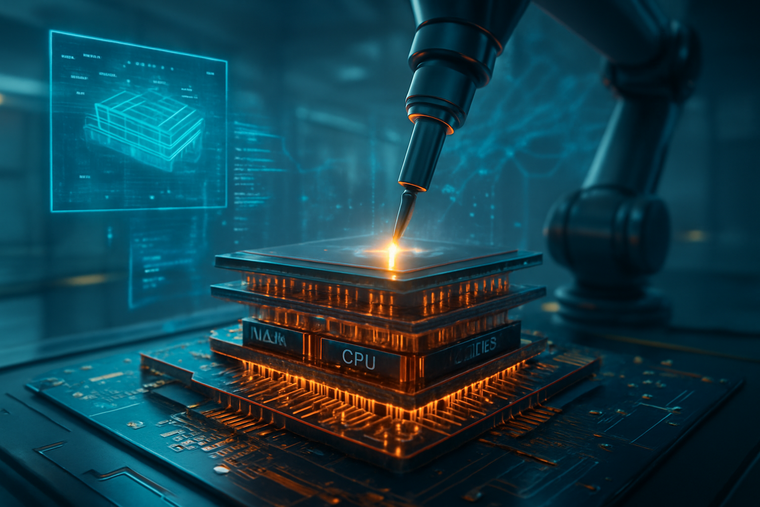
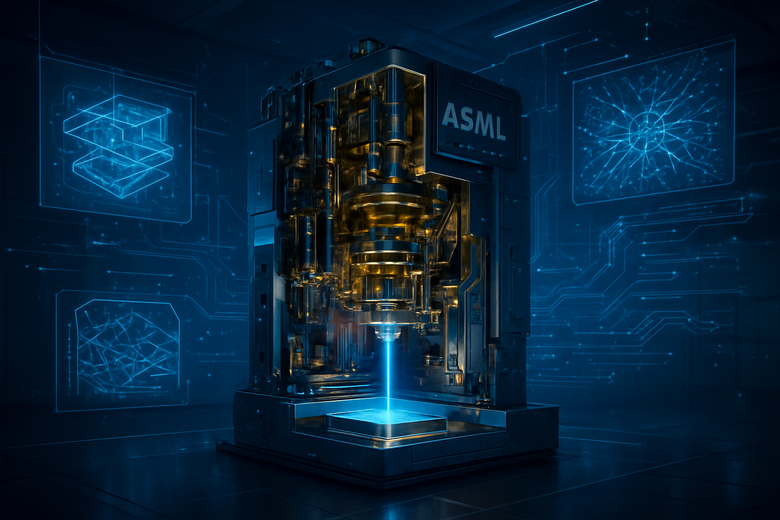
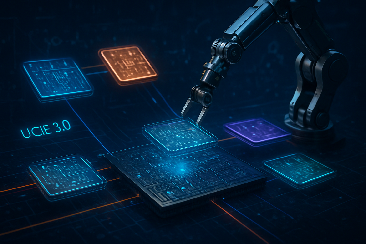
    The technical specifications of TSMC's offerings are critical to its lead. Its 3nm node (N3) and 5nm node (N5) are currently foundational for many flagship devices and AI chips, contributing 23% and a significant portion of its Q3 2025 wafer revenue, respectively. The transition to 2nm (N2) will further enhance transistor density and performance, crucial for the increasingly complex demands of AI models and data centers, promising a 15% performance gain and a 30% reduction in power consumption compared to the 3nm process. Furthermore, TSMC's advanced packaging technologies, such as CoWoS (Chip-on-Wafer-on-Substrate), are pivotal. CoWoS integrates logic silicon with high-bandwidth memory (HBM), a critical requirement for AI accelerators, effectively addressing current supply bottlenecks and offering a competitive edge that few can replicate at scale. CoWoS capacity is projected to reach 70,000 to 80,000 wafers per month by late 2025, and potentially 120,000 to 130,000 wafers per month by the end of 2026.

    This comprehensive suite of manufacturing and packaging solutions differentiates TSMC significantly from previous approaches and existing technologies, which often lack the same level of integration, efficiency, or sheer production capacity. The company's relentless investment in research and development keeps it at the forefront of process technology, which is a critical competitive advantage. Initial reactions from the AI research community and industry experts consistently highlight TSMC's indispensable role, often citing its technology as the bedrock upon which future AI advancements will be built. TSMC's mastery of these advanced processes and packaging allows it to hold a commanding 71-72% of the global pure-play foundry market share as of Q2 and Q3 2025, consistently staying above 64% throughout 2024 and 2025.

    Financially, TSMC has demonstrated exceptional performance throughout 2025. Revenue surged by approximately 39% year-over-year in Q2 2025 to ~US$29.4 billion, and jumped 30% to $32.30 billion in Q3 2025, reflecting a 40.8% year-over-year increase. For October 2025, net revenue rose 16.9% compared to October 2024, reaching NT$367.47 billion, and from January to October 2025, total revenue grew a substantial 33.8%. Consolidated revenue for November 2025 was NT$343.61 billion, up 24.5% year-over-year, contributing to a 32.8% year-to-date increase from January to November 2025. The company reported a record-high net profit for Q3 2025, reaching T$452.30 billion ($14.75 billion), surpassing analyst estimates, with a gross margin of an impressive 59.5%. AI and HPC are the primary catalysts for this growth, with AI-related applications alone accounting for 60% of TSMC's Q2 2025 revenue.

    A Linchpin for Innovation: How TSMC Shapes the Global Tech Ecosystem

    TSMC's manufacturing dominance in late 2025 has a profound and differentiated impact across the entire technology industry, acting as a critical enabler for cutting-edge AI, high-performance computing (HPC), and advanced mobile technologies. Its leadership dictates access to leading-edge silicon, influences competitive landscapes, and accelerates disruptive innovations. Major tech giants and AI powerhouses are critically dependent on TSMC for their most advanced chips. Companies like Apple (NASDAQ: AAPL), Nvidia (NASDAQ: NVDA), AMD (NASDAQ: AMD), Qualcomm (NASDAQ: QCOM), Google (NASDAQ: GOOGL), Microsoft (NASDAQ: MSFT), and Amazon (NASDAQ: AMZN) all leverage TSMC's 3nm and 2nm nodes, as well as its advanced packaging solutions like CoWoS, to create the high-performance, power-efficient processors essential for AI training and inference, high-end smartphones, and data center infrastructure. Nvidia, for instance, relies on TSMC for its AI GPUs, including the next-generation Blackwell chips, which are central to the AI revolution, while Apple consistently secures early access to new TSMC nodes for its flagship iPhone and Mac products, gaining a significant strategic advantage.

    For startups, however, TSMC's dominance presents a high barrier to entry. While its technology is vital, access to leading-edge nodes is expensive and often requires substantial volume commitments, making it difficult for smaller companies to compete for prime manufacturing slots. Fabless startups with innovative chip designs may find themselves constrained by TSMC's capacity limitations and pricing power, especially for advanced nodes where demand from tech giants is overwhelming. Lead times can be long, and early allocations for 2nm and 3nm are highly concentrated among a few major customers, which can significantly impact their time-to-market and cost structures. This creates a challenging environment where established players with deep pockets and long-standing relationships with TSMC often have a considerable competitive edge.

    The competitive landscape for other foundries is also significantly shaped by TSMC's lead. While rivals like Samsung Foundry (KRX: 005930) and Intel Foundry Services (NASDAQ: INTC) are aggressively investing to catch up, TSMC's technological moat, particularly in advanced nodes (7nm and below), remains substantial. Samsung has integrated Gate-All-Around (GAA) technology into its 3nm node and plans 2nm production in 2025, aiming to become an alternative, and Intel is focusing on its 18A process development. However, as of Q2 2025, Samsung holds a mere 7.3-9% of the pure foundry market, and Intel's foundry operation is still nascent compared to TSMC's behemoth scale. Due to TSMC's bottlenecks in advanced packaging (CoWoS) and front-end capacity at 3nm and 2nm, some fabless companies are exploring diversification; Tesla (NASDAQ: TSLA), for example, is reportedly splitting its next-generation Dojo AI6 chips between Samsung for front-end manufacturing and Intel for advanced packaging, highlighting a growing desire to mitigate reliance on a single supplier and suggesting a potential, albeit slow, shift in the industry's supply chain strategy.

    TSMC's advanced manufacturing capabilities are directly enabling the next wave of technological disruption across various sectors. The sheer power and efficiency of TSMC-fabricated AI chips are driving the development of entirely new AI applications, from more sophisticated generative AI models to advanced autonomous systems and highly intelligent edge devices. This also underpins the rise of "AI PCs," where advanced processors from companies like Qualcomm, Apple, and AMD, manufactured by TSMC, offer enhanced AI capabilities directly on the device, potentially shortening PC lifecycles and disrupting the market for traditional x86-based PCs. Furthermore, the demand for TSMC's advanced nodes and packaging is central to the massive investments by hyperscalers in AI infrastructure, transforming data centers to handle immense computational loads and potentially making older architectures less competitive.

    The Geopolitical Chessboard: TSMC's Wider Significance and Global Implications

    TSMC's dominance in late 2025 carries profound wider significance, acting as a pivotal enabler and, simultaneously, a critical bottleneck for the rapidly expanding artificial intelligence landscape. Its central role impacts AI trends, global economics, and geopolitics, while also raising notable concerns. The current AI landscape is characterized by an exponential surge in demand for increasingly powerful AI models—including large language models, complex neural networks, and applications in generative AI, cloud computing, and edge AI. This demand directly translates into a critical need for more advanced, efficient, and higher-density chips. TSMC's advancements in 3nm, 2nm, and future nodes, coupled with its advanced packaging solutions, are not merely incremental improvements but foundational enablers for the next generation of AI capabilities, allowing for the processing of more complex computations and larger datasets with unprecedented speed and energy efficiency.

    The impacts of TSMC's strong position on the AI industry are multifaceted. It accelerates the pace of innovation across various sectors, including autonomous vehicles, medical imaging, cloud computing, and consumer electronics, all of which increasingly depend on AI. Companies with strong relationships and guaranteed access to TSMC's advanced nodes, such as Nvidia and Apple, gain a substantial strategic advantage, crucial for maintaining their dominant positions in the AI hardware market. This can also create a widening gap between those who can leverage the latest silicon and those limited to less advanced processes, potentially impacting product performance, power efficiency, and time-to-market across the tech sector. Furthermore, TSMC's success significantly bolsters Taiwan's position as a technological powerhouse and has global implications for trade and supply chains.

    However, TSMC's dominance, while beneficial for technological advancement, also presents significant concerns, primarily geopolitical risks. The most prominent concern is the geopolitical instability in the Taiwan Strait, where tensions between China and Taiwan cast a long shadow. Any conflict or trade disruption could have catastrophic global consequences given TSMC's near-monopoly on advanced chip manufacturing. The "silicon shield" concept posits that global reliance on TSMC deters aggression, but also links Taiwan's fate to the world's access to technology. This concentration of advanced chip production in Taiwan creates extraordinary strategic vulnerability, as the global AI revolution depends on a highly concentrated supply chain involving Nvidia's designs, ASML's lithography equipment, and TSMC's manufacturing. Diversification efforts through new fabs in the US, Japan, and Germany aim to enhance resilience but face considerable costs and challenges, with Taiwan remaining the hub for the most advanced R&D and production.

    Comparing this era to previous AI milestones highlights the continuous importance of hardware. The current AI boom, particularly generative AI and large language models, is built upon the "foundational bedrock" of TSMC's advanced chips, much like the AI revival of the early 2000s was critically dependent on "exponential increases in computing power (especially GPUs) and the explosion of labeled data." Just as powerful computer hardware was vital then, TSMC's unprecedented computing power, efficiency, and density offered by its advanced nodes are enabling the scale and sophistication of modern AI that would be impossible otherwise. This situation underscores that cutting-edge chip manufacturing remains a critical enabler, pushing the boundaries of what AI can achieve and shaping the future trajectory of the entire field.

    The Road Ahead: Navigating the Future of Silicon and AI

    The semiconductor industry, with TSMC at its forefront, is poised for a period of intense growth and transformation, driven primarily by the burgeoning demand for Artificial Intelligence (AI) and High-Performance Computing (HPC). As of late 2025, both the broader industry and TSMC are navigating rapid technological advancements, evolving market dynamics, and significant geopolitical shifts. Near-term, the industry expects robust growth, with AI chips remaining the paramount driver, projected to surpass $150 billion in market value in 2025. Advanced packaging technologies like CoWoS and SoIC are crucial for continuing Moore's Law and enhancing chip performance for AI, with CoWoS production capacity expanding aggressively. The "2nm race" is a major focus, with TSMC's mass production largely on track for the second half of 2025, and an enhanced N2P version slated for 2026-2027, promising significant performance gains or power reductions. Furthermore, TSMC is accelerating the launch of its 1.6nm (A16) process by the end of 2026, which will introduce backside power delivery specifically targeting AI accelerators in data centers.

    Looking further ahead to 2028 and beyond, the global semiconductor market is projected to surpass $1 trillion by 2030 and potentially reach $2 trillion by 2040. This long-term growth will be fueled by continued miniaturization, with the industry aiming for 1.4nm (A14) by 2028 and 1nm (A10) nodes by 2030. TSMC is already constructing its A14 fab (Fab 25) as of October 2025, targeting significant performance improvements. 3D stacking and chiplets will become increasingly crucial for achieving higher transistor densities, with predictions of a trillion transistors on a single package by 2030. Research will focus on new materials, architectures, and next-generation lithography beyond current Extreme Ultraviolet (EUV) technology. Neuromorphic semiconductors, mimicking the human brain, are also being developed for increased power efficiency in AI and applications like humanoid robotics, promising a new frontier for AI hardware.

    However, this ambitious future is not without its challenges. Talent shortages remain a significant bottleneck for industry growth, with an estimated need for a million skilled workers by 2030. Geopolitical tensions and supply chain resilience continue to be major concerns, as export controls and shifting trade policies, particularly between the U.S. and China, reshape supply chain dynamics and make diversification a top priority. Rising manufacturing costs, with leading-edge fabs costing over $30 billion, also present a hurdle. For TSMC specifically, while its geographic expansion with new fabs in Arizona, Japan, and Germany aims to diversify its supply chain, Taiwan will remain the hub for the most advanced R&D and production, meaning geopolitical risks will persist. Increased competition from Intel, which is gaining momentum in advanced nodes (e.g., Intel 18A in 2025 and 1.4nm around 2026), could offer alternative manufacturing options for AI firms and potentially affect TSMC's market share in the long run.

    Experts view TSMC as the "unseen giant" powering the future of technology, indispensable due to its mastery of advanced process nodes, making it the sole producer of many sophisticated chips, particularly for AI and HPC. Analysts project that TSMC's earnings growth will accelerate, with free cash flow potentially reaching NT$3.27 trillion by 2035 and earnings per share possibly hitting $19.38 by 2030. Its strong client relationships with leading tech giants provide stable demand and insights into future technological needs, ensuring its business is seen as vital to virtually all technology, not just the AI boom, making it a robust long-term investment. What experts predict next is a continued race for smaller, more powerful nodes, further integration of advanced packaging, and an increasing focus on energy efficiency and sustainability as the industry scales to meet the insatiable demands of AI.

    The Indispensable Architect: A Concluding Perspective on TSMC's Enduring Impact

    As of late 2025, Taiwan Semiconductor Manufacturing Company (NYSE: TSM) stands as an undisputed titan in the semiconductor industry, cementing its pivotal role in powering the global technological landscape, particularly the burgeoning Artificial Intelligence (AI) sector. Its relentless pursuit of advanced manufacturing nodes and sophisticated packaging technologies has made it an indispensable partner for the world's leading tech innovators. Key takeaways from TSMC's current standing include its unrivaled foundry dominance, commanding approximately 70-72% of the global pure-play market, and its leadership in cutting-edge technology, with 3nm production ramping up and the highly anticipated 2nm process on track for mass production in late 2025. This technological prowess makes TSMC indispensable to AI chip manufacturing, serving as the primary producer for the world's most sophisticated AI chips from companies like Nvidia, Apple, AMD, and Qualcomm. This is further bolstered by robust financial performance and significant capital expenditures aimed at global expansion and technological advancement.

    TSMC's significance in AI history cannot be overstated; it is not merely a chip manufacturer but a co-architect of the AI future, providing the foundational processing power that fuels everything from large language models to autonomous systems. Historically, TSMC's continuous push for smaller, more efficient transistors and advanced packaging has been essential for every wave of AI innovation, enabling breakthroughs like the powerful GPUs crucial for the deep learning revolution. Its ability to consistently deliver leading-edge process nodes has allowed chip designers to translate architectural innovations into silicon, pushing the boundaries of what AI can achieve and marking a new era of interdependence between chip manufacturing and AI development.

    Looking long-term, TSMC's impact will continue to shape global technological leadership, economic competitiveness, and geopolitical dynamics. Its sustained dominance in advanced chip manufacturing is likely to ensure its central role in future technological advancements, especially as AI continues to expand into diverse applications such as 5G connectivity, electric and autonomous vehicles, and renewable energy. However, this dominance also brings inherent risks and challenges. Geopolitical tensions, particularly regarding the Taiwan Strait, pose significant downside threats, as any interruption to Taiwan's semiconductor sector could have serious global implications. While TSMC is actively diversifying its manufacturing footprint with fabs in the US, Japan, and Germany, Taiwan remains the critical node for the most advanced chip production, maintaining a technological lead that rivals have yet to match. The sheer difficulty and time required to establish advanced semiconductor manufacturing create a formidable moat for TSMC, reinforcing its enduring importance despite competitive efforts from Samsung and Intel.

    In the coming weeks and months, several key areas warrant close observation. The actual mass production rollout and yield rates of TSMC's 2nm (N2) process, scheduled for late Q4 2025, will be critical, as will updates on customer adoption from major clients. Progress on overseas fab construction in Arizona, Japan, and Germany will indicate global supply chain resilience. TSMC's ability to ramp up its CoWoS and next-generation CoPoS (Co-packaged Optics) packaging capacity will be crucial, as this remains a bottleneck for high-performance AI accelerators. Furthermore, watching for updates on TSMC's capital expenditure plans for 2026, proposed price hikes for N2 and N3 wafers, competitive moves by Samsung and Intel, and any shifts in geopolitical developments, especially regarding the Taiwan Strait and US-China trade policies, will provide immediate insights into the trajectory of this indispensable industry leader. TSMC's December sales and revenue release on January 8, 2026, and its Q4 2025 earnings projected for January 14, 2026, will offer immediate financial insights into these trends.


    This content is intended for informational purposes only and represents analysis of current AI developments.

    TokenRing AI delivers enterprise-grade solutions for multi-agent AI workflow orchestration, AI-powered development tools, and seamless remote collaboration platforms.
    For more information, visit https://www.tokenring.ai/.