Tag: TSMC

  • TSMC’s Unstoppable Momentum: Billions Poured into Global Expansion as AI Fuels Investor Frenzy

    TSMC’s Unstoppable Momentum: Billions Poured into Global Expansion as AI Fuels Investor Frenzy

    Taiwan Semiconductor Manufacturing Company (NYSE: TSM), the undisputed titan of the global semiconductor foundry industry, is experiencing an unprecedented surge in investment and investor confidence as of November 2025. Driven by an insatiable demand for cutting-edge chips powering the artificial intelligence revolution, TSMC is aggressively expanding its manufacturing footprint and technological capabilities worldwide, solidifying its indispensable role in the digital economy. This wave of capital expenditure and robust financial performance underscores the company's critical importance in shaping the future of technology.

    The immediate significance of TSMC's current trajectory cannot be overstated. With projected capital expenditures for 2025 ranging between $38 billion and $42 billion, the company is making a clear statement of intent: to maintain its technological leadership and meet the escalating global demand for advanced semiconductors. This substantial investment is primarily directed towards advanced process development, ensuring TSMC remains at the forefront of chip manufacturing, a position that is increasingly vital for tech giants and innovative startups alike.

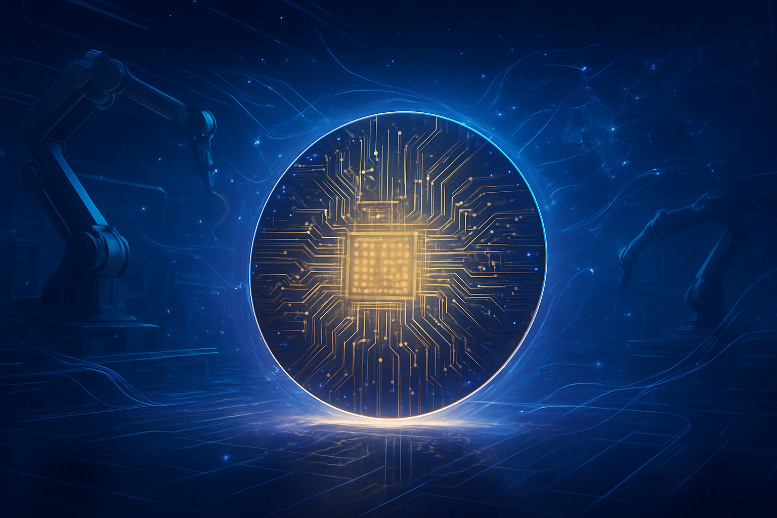
    Engineering the Future: TSMC's Technological Edge and Strategic Investments

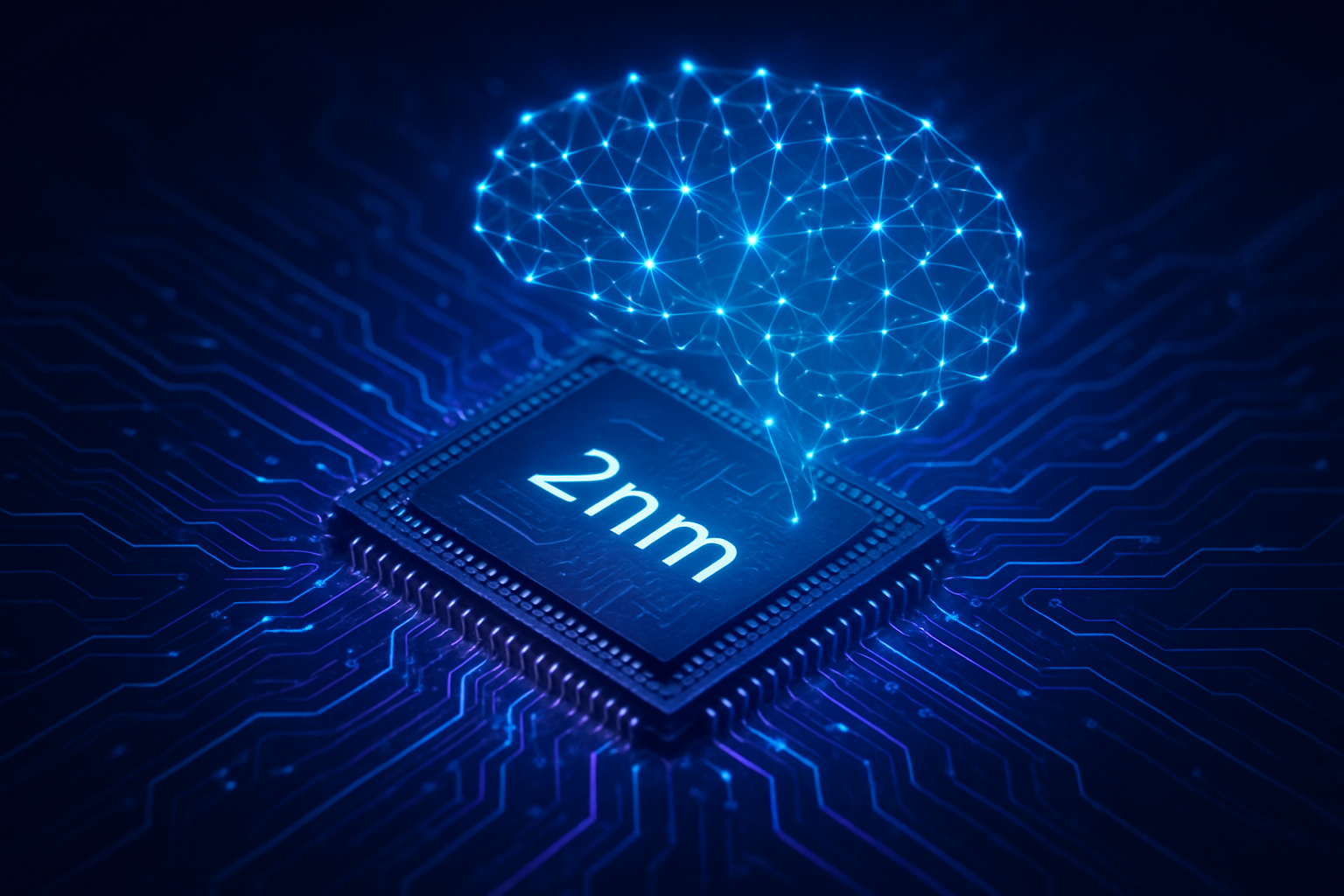
    TSMC's strategic investment initiatives are meticulously designed to reinforce its technological dominance and cater to the evolving needs of the high-performance computing (HPC) and AI sectors. Approximately 70% of its massive capital expenditure is funneled into advanced process development, with a significant portion dedicated to bringing 2-nanometer (nm) technology to mass production. The company anticipates commencing mass production of 2nm chips in the second half of 2025, with an ambitious target of reaching a monthly production capacity of up to 90,000 wafers by late 2026. This technological leap promises a 25-30% improvement in energy efficiency, a critical factor for power-hungry AI applications, and is expected to further boost TSMC's margins and secure long-term contracts.

    Beyond process node advancements, TSMC is also aggressively scaling its advanced packaging capabilities, recognizing their crucial role in integrating complex AI and HPC chips. Its Chip-on-Wafer-on-Substrate (CoWoS) capacity is projected to expand by over 80% from 2022 to 2026, while its System-on-Integrated-Chip (SoIC) capacity is expected to grow at a compound annual growth rate (CAGR) exceeding 100% during the same period. These packaging innovations are vital for overcoming the physical limitations of traditional chip design, allowing for denser, more powerful, and more efficient integration of components—a key differentiator from previous approaches and a necessity for the next generation of AI hardware.

    The company's global footprint expansion is equally ambitious. In Taiwan, seven new facilities are slated for 2025, including 2nm production bases in Hsinchu and Kaohsiung, and advanced packaging facilities across Tainan, Taichung, and Chiayi. Internationally, TSMC is dramatically increasing its investment in the United States to a staggering total of US$165 billion, establishing three new fabrication plants, two advanced packaging facilities, and a major R&D center in Phoenix, Arizona. Construction of its second Kumamoto fab in Japan is set to begin in Q1 2025, with mass production targeted for 2027, and progress continues on a new fab in Dresden, Germany. These expansions demonstrate a commitment to diversify its manufacturing base while maintaining its technological lead, a strategy that sets it apart from competitors who often struggle to match the scale and complexity of TSMC's advanced manufacturing.

    The AI Engine: How TSMC's Dominance Shapes the Tech Landscape

    TSMC's unparalleled manufacturing capabilities are not just a technical marvel; they are the bedrock upon which the entire AI industry is built, profoundly impacting tech giants, AI companies, and startups alike. Companies like Apple (NASDAQ: AAPL), NVIDIA (NASDAQ: NVDA), Advanced Micro Devices (NASDAQ: AMD), Broadcom (NASDAQ: AVGO), and Qualcomm (NASDAQ: QCOM) are heavily reliant on TSMC for the production of their most advanced semiconductors. This dependence means that TSMC's technological advancements and production capacity directly dictate the pace of innovation and product launches for these industry leaders.

    For major AI labs and tech companies, TSMC's leading-edge process technologies are critical enablers. The company's 3nm chips currently power Apple's latest devices, and its upcoming 2nm technology is expected to be crucial for the next generation of AI accelerators and high-performance processors. This ensures that companies at the forefront of AI development have access to the most power-efficient and high-performing chips, giving them a competitive edge. Without TSMC's capabilities, the rapid advancements seen in areas like large language models, autonomous systems, and advanced graphics processing would be significantly hampered.

    The competitive implications are clear: companies with strong partnerships and allocation at TSMC stand to benefit immensely. This creates a strategic advantage for those who can secure manufacturing slots for their innovative chip designs. Conversely, any disruption or bottleneck at TSMC could have cascading effects across the entire tech ecosystem, impacting product availability, development timelines, and market positioning. TSMC's consistent delivery and technological leadership minimize such risks, providing a stable and advanced manufacturing partner that is essential for the sustained growth of the AI and tech sectors.

    Global Geopolitics and the Silicon Backbone: Wider Significance of TSMC

    TSMC's role extends far beyond merely manufacturing chips; it is a linchpin of global technology, intertwining with geopolitical stability, economic prosperity, and the broader trajectory of technological advancement. The company's unchallenged market leadership, commanding an estimated 70% of the global chip manufacturing market and over 55% of the foundry sector in 2024, makes it a critical component of international supply chains. This technological indispensability means that major world economies and their leading tech firms are deeply invested in TSMC's success and stability.

    The company's extensive investments and global expansion efforts, particularly in the United States, Japan, and Europe, are not just about increasing capacity; they are strategic moves to de-risk supply chains and foster localized semiconductor ecosystems. The expanded investment in the U.S. alone is projected to create 40,000 construction jobs and tens of thousands of high-paying, high-tech manufacturing and R&D positions, driving over $200 billion of indirect economic output. This demonstrates the profound economic ripple effect of TSMC's operations and its significant contribution to global employment and innovation.

    Concerns about geopolitical tensions, particularly in the Taiwan Strait, inevitably cast a shadow over TSMC's valuation. However, the global reliance on its manufacturing capabilities acts as a mitigating factor, making its stability a shared international interest. The company's consistent innovation, as recognized by the Robert N. Noyce Award presented to its Chairman C.C. Wei and former Chairman Mark Liu in November 2025, underscores its profound contributions to the semiconductor industry, comparable to previous milestones that defined eras of computing. TSMC's advancements are not just incremental; they are foundational, enabling the current AI boom and setting the stage for future technological breakthroughs.

    The Road Ahead: Future Developments and Enduring Challenges

    Looking ahead, TSMC's trajectory is marked by continued aggressive expansion and relentless pursuit of next-generation technologies. The company's commitment to mass production of 2nm chips by the second half of 2025 and its ongoing research into even more advanced nodes signal a clear path towards sustained technological leadership. The planned construction of additional 2nm factories in Taiwan and the significant investments in advanced packaging facilities like CoWoS and SoIC are expected to further solidify its position as the go-to foundry for the most demanding AI and HPC applications.

    Potential applications and use cases on the horizon are vast, ranging from more powerful and efficient AI accelerators for data centers to advanced chips for autonomous vehicles, augmented reality devices, and ubiquitous IoT. Experts predict that TSMC's innovations will continue to push the boundaries of what's possible in computing, enabling new forms of intelligence and connectivity. The company's focus on energy efficiency in its next-generation processes is particularly crucial as AI workloads become increasingly resource-intensive, addressing a key challenge for sustainable technological growth.

    However, challenges remain. The immense capital expenditure required to stay ahead in the semiconductor race necessitates sustained profitability and access to talent. Geopolitical risks, while mitigated by global reliance, will continue to be a factor. Competition, though currently lagging in advanced nodes, could intensify in the long term. What experts predict will happen next is a continued arms race in semiconductor technology, with TSMC leading the charge, but also a growing emphasis on resilient supply chains and diversified manufacturing locations to mitigate global risks. The company's strategic global expansion is a direct response to these challenges, aiming to build a more robust and distributed manufacturing network.

    A Cornerstone of the AI Era: Wrapping Up TSMC's Impact

    In summary, TSMC's current investment trends and investor interest reflect its pivotal and increasingly indispensable role in the global technology landscape. Key takeaways include its massive capital expenditures directed towards advanced process nodes like 2nm and sophisticated packaging technologies, overwhelmingly positive investor sentiment fueled by robust financial performance and its critical role in the AI boom, and its strategic global expansion to meet demand and mitigate risks. The company's recent 17% increase in its quarterly dividend further signals confidence in its sustained growth and profitability.

    This development's significance in AI history is profound. TSMC is not just a manufacturer; it is the silent enabler of the AI revolution, providing the foundational hardware that powers everything from sophisticated algorithms to complex neural networks. Without its continuous innovation and manufacturing prowess, the rapid advancements in AI that we witness today would be severely constrained. Its technological leadership and market dominance make it a cornerstone of the modern digital age.

    Final thoughts on the long-term impact point to TSMC remaining a critical barometer for the health and direction of the tech industry. Its ability to navigate geopolitical complexities, maintain its technological edge, and continue its aggressive expansion will largely determine the pace of innovation for decades to come. What to watch for in the coming weeks and months includes further updates on its 2nm production ramp-up, progress on its global fab constructions, and any shifts in its capital expenditure guidance, all of which will provide further insights into the future of advanced semiconductor manufacturing and, by extension, the future of AI.


    This content is intended for informational purposes only and represents analysis of current AI developments.

    TokenRing AI delivers enterprise-grade solutions for multi-agent AI workflow orchestration, AI-powered development tools, and seamless remote collaboration platforms.
    For more information, visit https://www.tokenring.ai/.

  • Navigating the Nanometer Frontier: TSMC’s 2nm Process and the Shifting Sands of AI Chip Development

    Navigating the Nanometer Frontier: TSMC’s 2nm Process and the Shifting Sands of AI Chip Development

    The semiconductor industry is abuzz with speculation surrounding Taiwan Semiconductor Manufacturing Company's (TSMC) (NYSE: TSM) highly anticipated 2nm (N2) process node. Whispers from within the supply chain suggest that while N2 represents a significant leap forward in manufacturing technology, its power, performance, and area (PPA) improvements might be more incremental than the dramatic generational gains seen in the past. This nuanced advancement has profound implications, particularly for major clients like Apple (NASDAQ: AAPL) and the burgeoning field of next-generation AI chip development, where every nanometer and every watt counts.

    As the industry grapples with the escalating costs of advanced silicon, the perceived moderation in N2's PPA gains could reshape strategic decisions for tech giants. While some reports suggest this might lead to less astronomical cost increases per wafer, others indicate N2 wafers will still be significantly pricier. Regardless, the transition to N2, slated for mass production in the second half of 2025 with strong demand already reported for 2026, marks a pivotal moment, introducing Gate-All-Around (GAAFET) transistors and intensifying the race among leading foundries like Samsung and Intel to dominate the sub-3nm era. The efficiency gains, even if incremental, are critical for AI data centers facing unprecedented power consumption challenges.

    The Architectural Leap: GAAFETs and Nuanced PPA Gains Define TSMC's N2

    TSMC's 2nm (N2) process node, slated for mass production in the second half of 2025 following risk production commencement in July 2024, represents a monumental architectural shift for the foundry. For the first time, TSMC is moving away from the long-standing FinFET (Fin Field-Effect Transistor) architecture, which has dominated advanced nodes for over a decade, to embrace Gate-All-Around (GAAFET) nanosheet transistors. This transition is not merely an evolutionary step but a fundamental re-engineering of the transistor structure, crucial for continued scaling and performance enhancements in the sub-3nm era.

    In FinFETs, the gate controls the current flow by wrapping around three sides of a vertical silicon fin. While a significant improvement over planar transistors, GAAFETs offer superior electrostatic control by completely encircling horizontally stacked silicon nanosheets that form the transistor channel. This full encirclement leads to several critical advantages: significantly reduced leakage current, improved current drive, and the ability to operate at lower voltages, all contributing to enhanced power efficiency—a paramount concern for modern high-performance computing (HPC) and AI workloads. Furthermore, GAA nanosheets offer design flexibility, allowing engineers to adjust channel widths to optimize for specific performance or power targets, a feature TSMC terms NanoFlex.

    Despite some initial rumors suggesting limited PPA improvements, TSMC's official projections indicate robust gains over its 3nm N3E node. N2 is expected to deliver a 10% to 15% speed improvement at the same power consumption, or a 25% to 30% reduction in power consumption at the same speed. The transistor density is projected to increase by 15% (1.15x) compared to N3E. Subsequent iterations like N2P promise even further enhancements, with an 18% speed improvement and a 36% power reduction. These gains are further bolstered by innovations like barrier-free tungsten wiring, which reduces resistance by 20% in the middle-of-line (MoL).

    The AI research community and industry experts have reacted with "unprecedented" demand for N2, particularly from the HPC and AI sectors. Over 15 major customers, with about 10 focused on AI applications, have committed to N2. This signals a clear shift where AI's insatiable computational needs are now the primary driver for cutting-edge chip technology, surpassing even smartphones. Companies like NVIDIA (NASDAQ: NVDA), AMD (NASDAQ: AMD), Apple (NASDAQ: AAPL), Qualcomm (NASDAQ: QCOM), and others are heavily invested, recognizing that N2's significant power reduction capabilities (30-40%) are vital for mitigating the escalating electricity demands of AI data centers. Initial defect density and SRAM yield rates for N2 are reportedly strong, indicating a smooth path towards volume production and reinforcing industry confidence in this pivotal node.

    The AI Imperative: N2's Influence on Next-Gen Processors and Competitive Dynamics

    The technical specifications and cost implications of TSMC's N2 process are poised to profoundly influence the product roadmaps and competitive strategies of major AI chip developers, including Apple (NASDAQ: AAPL) and Qualcomm (NASDAQ: QCOM). While the N2 node promises substantial PPA improvements—a 10-15% speed increase or 25-30% power reduction, alongside a 15% transistor density boost over N3E—these advancements come at a significant price, with N2 wafers projected to cost between $30,000 and $33,000, a potential 66% hike over N3 wafers. This financial reality is shaping how companies approach their next-generation AI silicon.

    For Apple, a perennial alpha customer for TSMC's most advanced nodes, N2 is critical for extending its leadership in on-device AI. The A20 chip, anticipated for the iPhone 18 series in 2026, and future M-series processors (like the M5) for Macs, are expected to leverage N2. These chips will power increasingly sophisticated on-device AI capabilities, from enhanced computational photography to advanced natural language processing. Apple has reportedly secured nearly half of the initial N2 production, ensuring its premium devices maintain a cutting edge. However, the high wafer costs might lead to a tiered adoption, with only Pro models initially featuring the 2nm silicon, impacting the broader market penetration of this advanced technology. Apple's deep integration with TSMC, including collaboration on future 1.4nm nodes, underscores its commitment to maintaining a leading position in silicon innovation.

    Qualcomm (NASDAQ: QCOM), a dominant force in the Android ecosystem, is taking a more diversified and aggressive approach. Rumors suggest Qualcomm intends to bypass the standard N2 node and move directly to TSMC's more advanced N2P process for its Snapdragon 8 Elite Gen 6 and Gen 7 chipsets, expected in 2026. This strategy aims to "squeeze every last bit of performance" for its on-device Generative AI capabilities, crucial for maintaining competitiveness against rivals. Simultaneously, Qualcomm is actively validating Samsung Foundry's (KRX: 005930) 2nm process (SF2) for its upcoming Snapdragon 8 Elite 2 chip. This dual-sourcing strategy mitigates reliance on a single foundry, enhances supply chain resilience, and provides leverage in negotiations, a prudent move given the increasing geopolitical and economic complexities of semiconductor manufacturing.

    Beyond these mobile giants, the impact of N2 reverberates across the entire AI landscape. High-Performance Computing (HPC) and AI sectors are the primary drivers of N2 demand, with approximately 10 of the 15 major N2 clients being HPC-oriented. Companies like NVIDIA (NASDAQ: NVDA) for its Rubin Ultra GPUs and AMD (NASDAQ: AMD) for its Instinct MI450 accelerators are poised to leverage N2 for their next-generation AI chips, demanding unparalleled computational power and efficiency. Hyperscalers such as Google (NASDAQ: GOOGL), Amazon (NASDAQ: AMZN), and OpenAI are also designing custom AI ASICs that will undoubtedly benefit from the PPA advantages of N2. The intense competition also highlights the efforts of Intel Foundry (NASDAQ: INTC), whose 18A (1.8nm-class) process, featuring RibbonFET (GAA) and PowerVia (backside power delivery), is positioned as a strong contender, aiming for mass production by late 2025 or early 2026 and potentially offering unique advantages that TSMC won't implement until its A16 node.

    Beyond the Nanometer: N2's Broader Impact on AI Supremacy and Global Dynamics

    TSMC's 2nm (N2) process technology, with its groundbreaking transition to Gate-All-Around (GAAFET) transistors and significant PPA improvements, extends far beyond mere chip specifications; it profoundly influences the global race for AI supremacy and the broader semiconductor industry's strategic landscape. The N2 node, set for mass production in late 2025, is poised to be a critical enabler for the next generation of AI, particularly for increasingly complex models like large language models (LLMs) and generative AI, demanding unprecedented computational power.

    The PPA gains offered by N2—a 10-15% performance boost at constant power or 25-30% power reduction at constant speed compared to N3E, alongside a 15% increase in transistor density—are vital for extending Moore's Law and fueling AI innovation. The adoption of GAAFETs, a fundamental architectural shift from FinFETs, provides the fundamental control necessary for transistors at this scale, and the subsequent iterations like N2P and A16, incorporating backside power delivery, will further optimize these gains. For AI, where every watt saved and every transistor added contributes directly to the speed and efficiency of training and inference, N2 is not just an upgrade; it's a necessity.

    However, this advancement comes with significant concerns. The cost of N2 wafers is projected to be TSMC's most expensive yet, potentially exceeding $30,000 per wafer—a substantial increase that will inevitably be passed on to consumers. This exponential rise in manufacturing costs, driven by immense R&D and capital expenditure for GAAFET technology and extensive Extreme Ultraviolet (EUV) lithography steps, poses a challenge for market accessibility and could lead to higher prices for next-generation products. The complexity of the N2 process also introduces new manufacturing hurdles, requiring sophisticated design and production techniques.

    Furthermore, the concentration of advanced manufacturing capabilities, predominantly in Taiwan, raises critical supply chain concerns. Geopolitical tensions pose a tangible threat to the global semiconductor supply, underscoring the strategic importance of advanced chip production for national security and economic stability. While TSMC is expanding its global footprint with new fabs in Arizona and Japan, Taiwan remains the epicenter of its most advanced operations, highlighting the need for continued diversification and resilience in the global semiconductor ecosystem.

    Crucially, N2 addresses one of the most pressing challenges facing the AI industry: energy consumption. AI data centers are becoming enormous power hogs, with global electricity use projected to more double by 2030, largely driven by AI workloads. The 25-30% power reduction offered by N2 chips is essential for mitigating this escalating energy demand, allowing for more powerful AI compute within existing power envelopes and reducing the carbon footprint of data centers. This focus on efficiency, coupled with advancements in packaging technologies like System-on-Wafer-X (SoW-X) that integrate multiple chips and optical interconnects, is vital for overcoming the "fundamental physical problem" of moving data and managing heat in the era of increasingly powerful AI.

    The Road Ahead: N2 Variants, 1.4nm, and the AI-Driven Semiconductor Horizon

    The introduction of TSMC's 2nm (N2) process node in the second half of 2025 marks not an endpoint, but a new beginning in the relentless pursuit of semiconductor advancement. This foundational GAAFET-based node is merely the first step in a meticulously planned roadmap that includes several crucial variants and successor technologies, all geared towards sustaining the explosive growth of AI and high-performance computing.

    In the near term, TSMC is poised to introduce N2P in the second half of 2026, which will integrate backside power delivery. This innovative approach separates the power delivery network from the signal network, addressing resistance challenges and promising further improvements in transistor performance and power consumption. Following closely will be the A16 process, also expected in the latter half of 2026, featuring a Superpower Rail Delivery (SPR) nanosheet for backside power delivery. A16 is projected to offer an 8-10% performance boost and a 15-20% improvement in energy efficiency over N2 nodes, showcasing the rapid iteration inherent in advanced manufacturing.

    Looking further out, TSMC's roadmap extends to N2X, a high-performance variant tailored for High-Performance Computing (HPC) applications, anticipated for mass production in 2027. N2X will prioritize maximum clock speeds and voltage tolerance, making it ideal for the most demanding AI accelerators and server processors. Beyond 2nm, the industry is already looking towards 1.4nm production around 2027, with future nodes exploring even more radical technologies such as 2D materials, Complementary FETs (CFETs) that vertically stack transistors for ultimate density, and other novel GAA devices. Deep integration with advanced packaging techniques, such as chiplet designs, will become increasingly critical to continue scaling and enhancing system-level performance.

    These advanced nodes will unlock a new generation of applications. Flagship mobile SoCs from Apple (NASDAQ: AAPL), Qualcomm (NASDAQ: QCOM), and MediaTek (TPE: 2454) will leverage N2 for extended battery life and enhanced on-device AI capabilities. CPUs and GPUs from AMD (NASDAQ: AMD), NVIDIA (NASDAQ: NVDA), and Intel (NASDAQ: INTC) will utilize N2 for unprecedented AI acceleration in data centers and cloud computing, powering everything from large language models to complex scientific simulations. The automotive industry, with its growing reliance on advanced semiconductors for autonomous driving and ADAS, will also be a significant beneficiary.

    However, the path forward is not without its challenges. The escalating cost of manufacturing remains a primary concern, with N2 wafers projected to exceed $30,000. This immense financial burden will continue to drive up the cost of high-end electronics. Achieving consistently high yields with novel architectures like GAAFETs is also paramount for cost-effective mass production. Furthermore, the relentless demand for power efficiency will necessitate continuous innovation, with backside power delivery in N2P and A16 directly addressing this by optimizing power delivery.

    Experts universally predict that AI will be the primary catalyst for explosive growth in the semiconductor industry. The AI chip market alone is projected to reach an estimated $323 billion by 2030, with the entire semiconductor industry approaching $1.3 trillion. TSMC is expected to solidify its lead in high-volume GAAFET manufacturing, setting new standards for power efficiency, particularly in mobile and AI compute. Its dominance in advanced nodes, coupled with investments in advanced packaging solutions like CoWoS, will be crucial. While competition from Intel's 18A and Samsung's SF2 will remain fierce, TSMC's strategic positioning and technological prowess are set to define the next era of AI-driven silicon innovation.

    Comprehensive Wrap-up: TSMC's N2 — A Defining Moment for AI's Future

    The rumors surrounding TSMC's 2nm (N2) process, particularly the initial whispers of limited PPA improvements and the confirmed substantial cost increases, have catalyzed a critical re-evaluation within the semiconductor industry. What emerges is a nuanced picture: N2, with its pivotal transition to Gate-All-Around (GAAFET) transistors, undeniably represents a significant technological leap, offering tangible gains in power efficiency, performance, and transistor density. These improvements, even if deemed "incremental" compared to some past generational shifts, are absolutely essential for sustaining the exponential demands of modern artificial intelligence.

    The key takeaway is that N2 is less about a single, dramatic PPA breakthrough and more about a strategic architectural shift that enables continued scaling in the face of physical limitations. The move to GAAFETs provides the fundamental control necessary for transistors at this scale, and the subsequent iterations like N2P and A16, incorporating backside power delivery, will further optimize these gains. For AI, where every watt saved and every transistor added contributes directly to the speed and efficiency of training and inference, N2 is not just an upgrade; it's a necessity.

    This development underscores the growing dominance of AI and HPC as the primary drivers of advanced semiconductor manufacturing. Companies like Apple (NASDAQ: AAPL), Qualcomm (NASDAQ: QCOM), NVIDIA (NASDAQ: NVDA), and AMD (NASDAQ: AMD) are making strategic decisions—from early capacity reservations to diversified foundry approaches—to leverage N2's capabilities for their next-generation AI chips. The escalating costs, however, present a formidable challenge, potentially impacting product pricing and market accessibility.

    As the industry moves towards 1.4nm and beyond, the focus will intensify on overcoming these cost and complexity hurdles, while simultaneously addressing the critical issue of energy consumption in AI data centers. TSMC's N2 is a defining milestone, marking the point where architectural innovation and power efficiency become paramount. Its significance in AI history will be measured not just by its raw performance, but by its ability to enable the next wave of intelligent systems while navigating the complex economic and geopolitical landscape of global chip manufacturing.

    In the coming weeks and months, industry watchers will be keenly observing the N2 production ramp, initial yield rates, and the unveiling of specific products from key customers. The competitive dynamics between TSMC, Samsung, and Intel in the sub-2nm race will intensify, shaping the strategic alliances and supply chain resilience for years to come. The future of AI, inextricably linked to these nanometer-scale advancements, hinges on the successful and widespread adoption of technologies like TSMC's N2.


    This content is intended for informational purposes only and represents analysis of current AI developments.

    TokenRing AI delivers enterprise-grade solutions for multi-agent AI workflow orchestration, AI-powered development tools, and seamless remote collaboration platforms.
    For more information, visit https://www.tokenring.ai/.

  • Silicon Under Siege: TSMC Probes Alleged Trade Secret Heist, Sending Ripples Through AI Chip Race

    Silicon Under Siege: TSMC Probes Alleged Trade Secret Heist, Sending Ripples Through AI Chip Race

    The global semiconductor industry, the bedrock of modern artificial intelligence, is currently gripped by a high-stakes internal investigation at Taiwan Semiconductor Manufacturing Company (TSMC) (NYSE: TSM). The world's leading contract chip manufacturer is probing allegations that former senior executive Lo Wen-jen may have illicitly transferred critical trade secrets to rival Intel (NASDAQ: INTC) upon his departure. This unfolding drama, emerging in mid-November 2025, has immediately ignited concerns over intellectual property protection, national security, and the fiercely competitive landscape driving the future of AI chip development.

    At the heart of the matter are allegations that Lo Wen-jen, who retired from TSMC in July 2025 as its Senior Vice President of Corporate Strategy Development before joining Intel in late October 2025, may have improperly taken confidential information. Taiwanese media reports suggest the alleged secrets pertain to TSMC's most advanced process technologies, including the N2, A16, and A14 nodes, which are absolutely crucial for manufacturing next-generation AI accelerators and high-performance computing (HPC) chips. The incident underscores the immense value placed on technological leadership in an era where AI innovation is directly tied to cutting-edge silicon.

    The Microscopic Battleground: Unpacking TSMC's Next-Gen Process Technologies

    The alleged trade secret theft targets the very core of TSMC's technological prowess, focusing on process technologies that define the leading edge of chip manufacturing. These nodes, N2, A16, A14, and potentially even post-A14 developments, are pivotal for the continued advancement of artificial intelligence and high-performance computing.

    The N2 process technology represents TSMC's critical transition to the 2-nanometer class, marking a shift from FinFET to Gate-All-Around (GAAFET) architecture. N2 is the first TSMC node to adopt GAA nanosheet transistors, offering superior electrostatic control and significantly reduced leakage currents compared to previous FinFET designs. This translates to an impressive 15% performance gain at the same power or a 30-35% power reduction at the same speed compared to N3E, alongside a 1.15 times increase in logic density. Risk production for N2 began in July 2024, with high-volume manufacturing (HVM) anticipated in late 2025.

    Following N2, the A16 process technology ushers in TSMC's "Angstrom-class" era. While it maintains the GAAFET nanosheet architecture, A16 introduces a revolutionary Super Power Rail (SPR) Backside Power Delivery Network (BSPDN). This innovation routes all power through the backside of the chip, freeing up front-side resources for signal routing, thereby improving logic density, reducing IR drop, and enhancing power delivery efficiency. A16 is projected to deliver an 8-10% speed improvement or a 15-20% power reduction compared to N2P, with volume production slated for the second half of 2026.

    The A14 process technology, with HVM planned for 2028, represents the second generation of TSMC's GAAFETs. It leverages refined nanosheet stacking and channel control for enhanced performance, power efficiency, and logic density (10-15% performance gain or 25-30% lower power consumption, and 20-23% higher logic density over N2). An A14P variant incorporating BSPDN is also planned for 2029. These advancements are critical for the ever-increasing demands of AI workloads, which require chips with higher transistor density, lower power consumption, and improved computational efficiency. Initial reactions from the AI research community and industry experts, while cautious given the ongoing investigation, highlight the potential for significant disruption if such foundational technical know-how were indeed illicitly transferred. While some experts believe TSMC's complex R&D structure makes full replication difficult, the leakage of even partial information could provide a substantial shortcut to competitors.

    Reshaping the AI Chip Battleground: Corporate Implications

    The alleged trade secret transfer from TSMC (NYSE: TSM) to Intel (NASDAQ: INTC) by Lo Wen-jen carries profound implications for the intensely competitive AI chip market, affecting tech giants, startups, and the broader AI ecosystem. The core of the dispute revolves around TSMC's highly advanced 2-nanometer (2nm), A16, A14, and post-A14 process technologies, which are critical for manufacturing next-generation AI and high-performance computing (HPC) chips.

    For TSMC (NYSE: TSM), the incident poses a direct threat to its primary competitive advantage: technological leadership in cutting-edge process nodes. As the undisputed global leader in contract chip manufacturing, with a projected market share of 66% in 2025, any erosion of its technological lead could impact future revenue and market share, particularly in the high-growth AI chip segment. This situation underscores the vulnerability of even highly secure intellectual property and necessitates even more stringent internal security protocols. TSMC has already initiated legal action and internal investigations, emphasizing its "zero-tolerance policy" on IP violations.

    Conversely, for Intel (NASDAQ: INTC), which has historically lagged behind TSMC in advanced manufacturing processes, the alleged acquisition of TSMC's 2nm, A16, and A14 process data could significantly accelerate its foundry roadmap. This could potentially allow Intel to close the technology gap much faster than anticipated, bolstering its competitive positioning and making it a more viable alternative for AI chip manufacturing and potentially attracting major clients like Nvidia (NASDAQ: NVDA) and AMD (NASDAQ: AMD), who currently rely heavily on TSMC. Intel's CEO has publicly denied the allegations, stating the company respects intellectual property, but the mere possibility of such a transfer has already impacted market perceptions, with Intel's shares reportedly experiencing a 4% decline following the initial news.

    The AI companies like Nvidia (NASDAQ: NVDA), which dominates the AI accelerator market, and AMD (NASDAQ: AMD), with its growing MI300 series, heavily rely on TSMC for manufacturing their most advanced AI GPUs. A compromise of TSMC's cutting-edge technology could indirectly affect these companies by potentially delaying future process node availability or increasing manufacturing costs if TSMC's competitive edge is weakened. However, if Intel rapidly advances its foundry capabilities, it could create a more competitive foundry market, offering more diversified supply options and potentially more favorable pricing. This could reduce the current over-reliance on TSMC, which could benefit cloud giants developing custom AI ASICs. For startups, any disruption to the supply of advanced AI chips from leading foundries could severely impact their ability to develop and scale AI solutions, though a more competitive foundry landscape could eventually lead to more accessible and diverse manufacturing options in the long term.

    A Broader Canvas: AI, National Security, and IP's Fragile Shield

    The alleged TSMC-Intel trade secret dispute transcends a mere corporate legal battle; it resonates across the broader AI landscape, touching upon critical issues of national security, technological sovereignty, and the ever-fragile shield of intellectual property protection within the semiconductor industry. This incident highlights the intense global race for advanced chip technology, which is not just an economic driver but a foundational element of national power and future AI capabilities.

    Advanced semiconductor manufacturing is the bedrock upon which modern AI is built. The insatiable demand for computational power in AI applications, driven by specialized chips, makes TSMC's role as the primary producer of the world's most sophisticated chips absolutely critical. If proven, the alleged transfer of TSMC's 2nm process technology secrets could significantly influence the competitive dynamics of the AI industry. The 2nm Gate-All-Around (GAA) transistor technology, central to next-generation AI and high-performance computing (HPC) markets, promises substantial performance and efficiency gains. A compromise of such foundational manufacturing know-how could theoretically accelerate a competitor's ability to produce more advanced AI chips, thereby disrupting the delicate balance of innovation and market leadership, impacting major players like Apple (NASDAQ: AAPL) and Nvidia (NASDAQ: NVDA).

    The dispute also carries profound implications for national security and technological sovereignty. Governments worldwide increasingly recognize semiconductors as strategic assets, essential for defense, cloud computing, space technology, and national infrastructure. Taiwan, as a crucial hub for advanced chip production, views its semiconductor industry as a matter of national security, evidenced by the involvement of its High Prosecutors Office in the probe under the amended National Security Act. This reflects a global trend where nations are investing heavily in domestic semiconductor production through initiatives like the US CHIPS and Science Act and the EU Chips Act, aiming to reduce reliance on foreign suppliers and secure their technological future in critical areas, including AI development.

    The incident underscores the perennial challenges of intellectual property protection in the semiconductor industry. Characterized by rapid innovation and astronomical R&D costs, IP—especially trade secrets—is a vital competitive advantage. Insider threats, as alleged in this case, remain a significant vulnerability. The economic cost of trade secret theft is staggering, estimated at 1-3% of GDP annually for developed economies. This case draws parallels to historical instances of high-stakes IP theft, such as the alleged transfer of self-driving car technology between Google (NASDAQ: GOOGL) (Waymo) and Uber, or the targeting of ASML's (AMS: ASML) computational lithography software. These events consistently demonstrate how the compromise of specialized foundational technology can have cascading effects, reshaping industry leadership and national power.

    The Road Ahead: Navigating the Future of Silicon and AI

    The ongoing TSMC-Intel trade secret investigation is poised to trigger significant near-term legal and corporate actions, reshape the competitive landscape for AI chips, drive new applications for advanced process technologies, highlight critical intellectual property (IP) protection challenges, and have profound long-term consequences for the global semiconductor industry.

    In the near term, several legal and corporate actions are expected. TSMC (NYSE: TSM) has launched an internal investigation and indicated plans for legal action based on its findings, while Taiwanese prosecutors are conducting a national security probe into Lo Wen-jen. Intel (NASDAQ: INTC) CEO Lip-Bu Tan has publicly dismissed the allegations, maintaining the company's respect for IP. This incident will likely lead to increased scrutiny over the movement of senior-level talent between competing semiconductor companies and could prompt new regulatory developments related to Taiwan's tech-security laws.

    Longer term, the dispute will inevitably influence the competitive dynamics for AI chips. TSMC's dominance in cutting-edge nodes, crucial for AI accelerators, has created a global manufacturing bottleneck. Intel, with its IDM 2.0 strategy and significant investments, aims to reclaim leadership in semiconductor manufacturing. If the allegations against Lo Wen-jen are substantiated, it could potentially provide competitors with insights into TSMC's proprietary methodologies, thereby disrupting the competitive balance and impacting chip availability, pricing, and overall technological leadership. Beyond corporate rivalry, geopolitical tensions continue to influence the global semiconductor landscape, pushing governments to invest in domestic production and self-sufficiency. Advanced process technologies, such as 3nm, 2nm, and smaller, are fundamental to the evolution of high-performance computing (HPC) and AI, enabling more powerful and efficient AI accelerators for complex AI training and inferencing. The increasing sophistication of AI applications will drive an even greater demand for advanced silicon, making the integrity of these technologies paramount.

    The investigation highlights the increasing criticality and vulnerability of intellectual property in the semiconductor industry. IP theft, driven by the desire to accelerate technological development without the substantial R&D costs, is a growing concern. Experts suggest that the outcome of this dispute will not only impact the corporate reputations of TSMC and Intel but could also profoundly shape the future of global chip innovation and supply. It underscores the "talent war" between these giants and the need for companies to clearly identify and comprehensively protect their IP assets, emphasizing strong internal governance and well-defined trade secret frameworks.

    Conclusion: A Defining Moment for the AI Era's Foundation

    The TSMC (NYSE: TSM) and Intel (NASDAQ: INTC) trade secret investigation represents a defining moment for the AI era's foundational technology. At its core, this incident underscores the immense value placed on intellectual property in the semiconductor industry, particularly as the world races to develop more powerful and efficient AI chips. The alleged transfer of critical manufacturing know-how, if proven, could significantly influence the competitive landscape, potentially accelerating one player's roadmap while challenging another's long-held technological lead.

    This development's significance in AI history cannot be overstated. Advanced silicon is the engine of artificial intelligence, powering everything from sophisticated large language models to autonomous systems. Any disruption or shift in the control of leading-edge chip manufacturing directly impacts the pace and direction of AI innovation globally. The involvement of the Taiwanese government, citing national security concerns, further elevates this from a corporate dispute to a geopolitical flashpoint, highlighting the strategic importance of semiconductor sovereignty in the 21st century.

    The long-term impact will likely include a renewed focus on robust IP protection strategies across the industry, potentially leading to more stringent employee non-compete clauses and enhanced digital security measures. The legal precedents set by Taiwanese prosecutors under the National Security Act could have far-reaching implications for protecting critical technological know-how. While TSMC's formidable ecosystem and continuous innovation are expected to provide resilience, the incident serves as a stark reminder of the vulnerabilities inherent in a globalized, highly competitive tech landscape.

    In the coming weeks and months, all eyes will be on the legal proceedings and formal charges, if any, brought against Lo Wen-jen. Corporate responses from both TSMC and Intel, including any civil lawsuits or internal policy changes, will be closely scrutinized. Market shifts, particularly any confirmed impact on TSMC's technology roadmap or Intel's accelerated advanced process development, will also be keenly watched by investors and industry analysts. This investigation is a critical barometer for the health of the semiconductor industry and its pivotal role in shaping the future of AI.


    This content is intended for informational purposes only and represents analysis of current AI developments.

    TokenRing AI delivers enterprise-grade solutions for multi-agent AI workflow orchestration, AI-powered development tools, and seamless remote collaboration platforms.
    For more information, visit https://www.tokenring.ai/.

  • Semiconductor Titans Ride AI Wave: A Financial Deep Dive into a Trillion-Dollar Horizon

    Semiconductor Titans Ride AI Wave: A Financial Deep Dive into a Trillion-Dollar Horizon

    The global semiconductor industry is experiencing an unprecedented boom in late 2025, largely propelled by the insatiable demand for Artificial Intelligence (AI) and High-Performance Computing (HPC). This surge is not merely a fleeting trend but a fundamental shift, positioning the sector on a trajectory to achieve an ambitious $1 trillion in annual chip sales by 2030. Companies at the forefront of this revolution are reporting record revenues and outlining aggressive expansion strategies, signaling a pivotal era for technological advancement and economic growth.

    This period marks a significant inflection point, as the foundational components of the digital age become increasingly sophisticated and indispensable. The immediate significance lies in the acceleration of AI development across all sectors, from data centers and cloud computing to advanced consumer electronics and autonomous vehicles. The financial performance of leading semiconductor firms reflects this robust demand, with projections indicating sustained double-digit growth for the foreseeable future.

    Unpacking the Engine of Innovation: Technical Prowess and Market Dynamics

    The semiconductor market is projected to expand significantly in 2025, with forecasts ranging from an 11% to 15% year-over-year increase, pushing the market size to approximately $697 billion to $700.9 billion. This momentum is set to continue into 2026, with an estimated 8.5% growth to $760.7 billion. Generative AI and data centers are the primary catalysts, with AI-related chips (GPUs, CPUs, HBM, DRAM, and advanced packaging) expected to generate a staggering $150 billion in sales in 2025. The Logic and Memory segments are leading this expansion, both projected for robust double-digit increases, while High-Bandwidth Memory (HBM) demand is particularly strong, with revenue expected to reach $21 billion in 2025, a 70% year-over-year increase.

    Technological advancements are at the heart of this growth. NVIDIA (NASDAQ: NVDA) continues to innovate with its Blackwell architecture and the upcoming Rubin platform, critical for driving future AI revenue streams. TSMC (NYSE: TSM) remains the undisputed leader in advanced process technology, mastering 3nm and 5nm production and rapidly expanding its CoWoS (chip-on-wafer-on-substrate) advanced packaging capacity, which is crucial for high-performance AI chips. Intel (NASDAQ: INTC), through its IDM 2.0 strategy, is aggressively pursuing process leadership with its Intel 18A and 14A processes, featuring innovations like RibbonFET (gate-all-around transistors) and PowerVia (backside power delivery), aiming to compete directly with leading foundries. AMD (NASDAQ: AMD) has launched an ambitious AI roadmap through 2027, introducing the MI350 GPU series with a 4x generational increase in AI compute and the forthcoming Helios rack-scale AI solution, promising up to 10x more AI performance.

    These advancements represent a significant departure from previous industry cycles, which were often driven by incremental improvements in general-purpose computing. Today's focus is on specialized AI accelerators, advanced packaging techniques, and a strategic diversification of foundry capabilities. The initial reaction from the AI research community and industry experts has been overwhelmingly positive, with reports of "Blackwell sales off the charts" and "cloud GPUs sold out," underscoring the intense demand for these cutting-edge solutions.

    The AI Arms Race: Competitive Implications and Market Positioning

    NVIDIA (NASDAQ: NVDA) stands as the undeniable titan in the AI hardware market. As of late 2025, it maintains a formidable lead, commanding over 80% of the AI accelerator market and powering more than 75% of the world's top supercomputers. Its dominance is fueled by relentless innovation in GPU architecture, such as the Blackwell series, and its comprehensive CUDA software ecosystem, which has become the de facto standard for AI development. NVIDIA's market capitalization hit $5 trillion in October 2025, at times making it the world's most valuable company, a testament to its strategic advantages and market positioning.

    TSMC (NYSE: TSM) plays an equally critical, albeit different, role. As the world's largest pure-play wafer foundry, TSMC captured 71% of the pure-foundry market in Q2 2025, driven by strong demand for AI and new smartphones. It is responsible for an estimated 90% of 3nm/5nm AI chip production, making it an indispensable partner for virtually all leading AI chip designers, including NVIDIA. TSMC's commitment to advanced packaging and geopolitical diversification, with new fabs being built in the U.S., further solidifies its strategic importance.

    Intel (NASDAQ: INTC), while playing catch-up in the discrete GPU market, is making a significant strategic pivot with its Intel Foundry Services (IFS) under the IDM 2.0 strategy. By aiming for process performance leadership by 2025 with its 18A process, Intel seeks to become a major foundry player, competing directly with TSMC and Samsung. This move could disrupt the existing foundry landscape and provide alternative supply chain options for AI companies. AMD (NASDAQ: AMD), with its aggressive AI roadmap, is directly challenging NVIDIA in the AI GPU space with its Instinct MI350 series and upcoming Helios rack solutions. While still holding a smaller share of the discrete GPU market (6% in Q2 2025), AMD's focus on high-performance AI compute positions it as a strong contender, potentially eroding some of NVIDIA's market dominance over time.

    A New Era: Wider Significance and Societal Impacts

    The current semiconductor boom, driven by AI, is more than just a financial success story; it represents a fundamental shift in the broader AI landscape and technological trends. The proliferation of AI-powered PCs, the expansion of data centers, and the rapid advancements in autonomous driving all hinge on the availability of increasingly powerful and efficient chips. This era is characterized by an unprecedented level of integration between hardware and software, where specialized silicon is designed specifically to accelerate AI workloads.

    The impacts are far-reaching, encompassing economic growth, job creation, and the acceleration of scientific discovery. However, this rapid expansion also brings potential concerns. Geopolitical tensions, particularly between the U.S. and China, and Taiwan's pivotal role in advanced chip production, introduce significant supply chain vulnerabilities. Export controls and tariffs are already impacting market dynamics, revenue, and production costs. In response, governments and industry stakeholders are investing heavily in domestic production capabilities and regional partnerships, such as the U.S. CHIPS and Science Act, to bolster resilience and diversify supply chains.

    Comparisons to previous AI milestones, such as the early days of deep learning or the rise of large language models, highlight the current period as a critical inflection point. The ability to efficiently train and deploy increasingly complex AI models is directly tied to the advancements in semiconductor technology. This symbiotic relationship ensures that progress in one area directly fuels the other, setting the stage for transformative changes across industries and society.

    The Road Ahead: Future Developments and Expert Predictions

    Looking ahead, the semiconductor industry is poised for continued innovation and expansion. Near-term developments will likely focus on further advancements in process nodes, with companies like Intel pushing the boundaries of 14A and beyond, and TSMC refining its next-generation technologies. The expansion of advanced packaging techniques, such as TSMC's CoWoS, will be crucial for integrating more powerful and efficient AI accelerators. The rise of AI PCs, expected to constitute 50% of PC shipments in 2025, signals a broad integration of AI capabilities into everyday computing, opening up new market segments.

    Long-term developments will likely include the proliferation of edge AI, where AI processing moves closer to the data source, reducing latency and enhancing privacy. This will necessitate the development of even more power-efficient and specialized chips. Potential applications on the horizon are vast, ranging from highly personalized AI assistants and fully autonomous systems to groundbreaking discoveries in medicine and materials science.

    However, significant challenges remain. Scaling production to meet ever-increasing demand, especially for advanced nodes and packaging, will require massive capital expenditures and skilled labor. Geopolitical stability will continue to be a critical factor, influencing supply chain strategies and international collaborations. Experts predict a continued period of intense competition and innovation, with a strong emphasis on full-stack solutions that combine cutting-edge hardware with robust software ecosystems. The industry will also need to address the environmental impact of chip manufacturing and the energy consumption of large-scale AI operations.

    A Pivotal Moment: Comprehensive Wrap-up and Future Watch

    The semiconductor industry in late 2025 is undergoing a profound transformation, driven by the relentless march of Artificial Intelligence. The key takeaways are clear: AI is the dominant force shaping market growth, leading companies like NVIDIA, TSMC, Intel, and AMD are making strategic investments and technological breakthroughs, and the global supply chain is adapting to new geopolitical realities.

    This period represents a pivotal moment in AI history, where the theoretical promises of artificial intelligence are being rapidly translated into tangible hardware capabilities. The current wave of innovation, marked by specialized AI accelerators and advanced manufacturing techniques, is setting the stage for the next generation of intelligent systems. The long-term impact will be nothing short of revolutionary, fundamentally altering how we interact with technology and how industries operate.

    In the coming weeks and months, market watchers should pay close attention to several key indicators. These include the financial reports of leading semiconductor companies, particularly their guidance on AI-related revenue; any new announcements regarding process technology advancements or advanced packaging solutions; and, crucially, developments in geopolitical relations that could impact supply chain stability. The race to power the AI future is in full swing, and the semiconductor titans are leading the charge.


    This content is intended for informational purposes only and represents analysis of current AI developments.

    TokenRing AI delivers enterprise-grade solutions for multi-agent AI workflow orchestration, AI-powered development tools, and seamless remote collaboration platforms.
    For more information, visit https://www.tokenring.ai/.

  • TSMC Rocked by Alleged 2nm and A16 Secret Leak: Former Executive Under Scrutiny

    Hsinchu, Taiwan – November 20, 2025 – Taiwan Semiconductor Manufacturing Company (TSMC) (NYSE: TSM), the world's leading contract chipmaker, finds itself embroiled in a high-stakes investigation following the suspected leak of its most advanced manufacturing secrets. The alleged breach centers on highly coveted 2-nanometer (2nm), A16, and A14 process technologies, critical for the next generation of high-performance computing and artificial intelligence. This incident has sent ripples through the global semiconductor industry, raising urgent questions about intellectual property protection and the intense competition for technological supremacy.

    The allegations primarily target Lo Wei-jen, a former Senior Vice President for Corporate Strategy Development at TSMC, who retired in July 2025 after a distinguished 21-year career with the company. Prosecutors officially launched an investigation on November 19, 2025, into claims that Lo Wei-jen may have taken confidential documents related to these cutting-edge processes, potentially transferring them to Intel (NASDAQ: INTC), a company he reportedly joined in late October 2025. This development comes on the heels of earlier internal suspicions at TSMC and a broader crackdown on industrial espionage in Taiwan's critical semiconductor sector.

    Unpacking the Alleged Breach: The Crown Jewels of Chipmaking at Risk

    The core of the alleged leak involves TSMC's 2nm, A16, and A14 process technologies, representing the pinnacle of semiconductor manufacturing. The 2nm process, in particular, is a game-changer, promising unprecedented transistor density, power efficiency, and performance gains crucial for powering advanced AI accelerators, high-end mobile processors, and data center infrastructure. These technologies are not merely incremental improvements; they are foundational advancements that dictate the future trajectory of computing power and innovation across industries.

    While specific technical specifications of the allegedly leaked information remain under wraps due to the ongoing investigation, the sheer significance of 2nm technology lies in its ability to pack more transistors into a smaller area, enabling more complex and powerful chips with reduced energy consumption. This leap in miniaturization is achieved through novel transistor architectures and advanced lithography techniques, differentiating it significantly from existing 3nm or 4nm processes currently in mass production. The A16 and A14 processes further extend this technological lead, indicating TSMC's roadmap for continued dominance. Initial reactions from the AI research community and industry experts, though cautious due to the lack of confirmed details, underscore the potential competitive advantage such information could confer. The consensus is that any insight into these proprietary processes could shave years off development cycles for competitors, particularly in the race to develop more powerful and efficient AI hardware.

    This incident differs markedly from typical employee departures, where knowledge transfer is often limited to general strategic insights. The allegations suggest a systematic attempt to extract detailed technical documentation, reportedly involving requests for comprehensive briefings on advanced technologies prior to retirement and the physical removal of a significant volume of data. This level of alleged misconduct points to a calculated effort to compromise TSMC's technological lead, rather than an incidental transfer of general expertise.

    Competitive Whirlwind: Reshaping the Semiconductor Landscape

    The potential leak of TSMC's 2nm, A16, and A14 process technologies carries profound implications for AI companies, tech giants, and startups alike. If the allegations prove true, Intel (NASDAQ: INTC), the company Lo Wei-jen allegedly joined, stands to potentially benefit from this development. Access to TSMC's advanced process know-how could significantly accelerate Intel's efforts to catch up in the foundry space and bolster its own manufacturing capabilities, particularly as it aims to reclaim its leadership in chip technology and become a major contract chipmaker. This could directly impact its ability to produce competitive AI chips and high-performance CPUs.

    The competitive implications for major AI labs and tech companies are immense. Companies like NVIDIA (NASDAQ: NVDA), Apple (NASDAQ: AAPL), and Qualcomm (QCOM), which rely heavily on TSMC's cutting-edge manufacturing for their AI accelerators and mobile processors, could face a more diversified and potentially more competitive foundry landscape in the long run. While TSMC's immediate market position as the dominant advanced foundry remains strong, any erosion of its unique technological advantage could lead to increased pressure on pricing and lead times. For startups in the AI hardware space, a more competitive foundry market could offer more options, but also introduces uncertainty regarding the future availability and pricing of the most advanced nodes.

    Potential disruption to existing products or services could manifest if competitors leverage the leaked information to rapidly close the technology gap, forcing TSMC's customers to reassess their supply chain strategies. This scenario could lead to a reshuffling of orders and a more fragmented market for advanced chip manufacturing. TSMC's strategic advantage has long been its unparalleled process technology leadership. A successful breach of these core secrets could undermine that advantage, impacting its market positioning and potentially altering the competitive dynamics between pure-play foundries and integrated device manufacturers (IDMs).

    Broader Ramifications: A Wake-Up Call for IP Protection

    This alleged leak fits into a broader, escalating trend of industrial espionage and intellectual property theft within the global technology sector, particularly concerning critical national technologies like semiconductors. Taiwan, a global leader in chip manufacturing, has been increasingly vigilant against such threats, especially given the geopolitical significance of its semiconductor industry. The incident underscores the immense value placed on advanced chipmaking know-how and the lengths to which competitors or state-backed actors might go to acquire it.

    The impacts extend beyond mere corporate competition. Such leaks raise significant concerns about supply chain security and national economic resilience. If core technologies of a critical industry leader like TSMC can be compromised, it could have cascading effects on global technology supply chains, impacting everything from consumer electronics to defense systems. This incident also draws comparisons to previous AI milestones and breakthroughs where proprietary algorithms or architectural designs were fiercely protected, highlighting that the battle for technological supremacy is fought not just in research labs but also in the realm of corporate espionage.

    Potential concerns include the long-term erosion of trust within the industry, increased costs for security measures, and a more protectionist stance from technology-leading nations. The incident serves as a stark reminder that as AI and other advanced technologies become more central to economic and national security, the safeguarding of the underlying intellectual property becomes paramount.

    The Road Ahead: Navigating Uncertainty and Bolstering Defenses

    In the near-term, the focus will be on the ongoing investigation by Taiwanese prosecutors. The outcome of this probe, including any indictments and potential legal ramifications for Lo Wei-jen and others involved, will be closely watched. TSMC is expected to double down on its internal security protocols and intellectual property protection measures, potentially implementing even stricter access controls, monitoring systems, and employee agreements. The company's "zero-tolerance policy" for IP violations will likely be reinforced with more robust enforcement mechanisms.

    Long-term developments could see a re-evaluation of industry practices regarding employee mobility, particularly for senior executives with access to highly sensitive information. There might be increased calls for stricter non-compete clauses and extended cooling-off periods for individuals transitioning between rival companies, especially across national borders. Potential applications and use cases on the horizon for TSMC include further advancements in 2nm and beyond, catering to the ever-increasing demands of AI and high-performance computing. However, challenges that need to be addressed include maintaining talent while preventing knowledge transfer, balancing innovation with security, and navigating a complex geopolitical landscape where technological leadership is a strategic asset.

    Experts predict that this incident will serve as a significant catalyst for the entire semiconductor industry to review and strengthen its IP protection strategies. It's also likely to intensify the global competition for top engineering talent, as companies seek to innovate internally while simultaneously safeguarding their existing technological advantages.

    A Critical Juncture for Semiconductor Security

    The suspected leak of TSMC's core technical secrets marks a critical juncture in the ongoing battle for technological supremacy in the semiconductor industry. The allegations against former executive Lo Wei-jen, involving the company's most advanced 2nm, A16, and A14 process technologies, underscore the immense value of intellectual property in today's high-tech landscape. The incident highlights not only the internal vulnerabilities faced by even the most secure companies but also the broader implications for national security and global supply chains.

    The significance of this development in AI history cannot be overstated. As AI applications become more sophisticated, they demand increasingly powerful and efficient underlying hardware. Any compromise of the foundational manufacturing processes that enable such hardware could have far-reaching consequences, potentially altering competitive dynamics, delaying technological progress, and impacting the availability of cutting-edge AI solutions.

    What to watch for in the coming weeks and months includes the progress of the judicial investigation, any official statements from TSMC or Intel, and the industry's response in terms of tightening security measures. This event serves as a potent reminder that in the race for AI dominance, the protection of intellectual property is as crucial as the innovation itself.


    This content is intended for informational purposes only and represents analysis of current AI developments.

    TokenRing AI delivers enterprise-grade solutions for multi-agent AI workflow orchestration, AI-powered development tools, and seamless remote collaboration platforms.
    For more information, visit https://www.tokenring.ai/.

  • TSMC’s Global Gambit: A $165 Billion Bet Reshaping the Semiconductor Landscape in the US and Japan

    TSMC’s Global Gambit: A $165 Billion Bet Reshaping the Semiconductor Landscape in the US and Japan

    Taiwan Semiconductor Manufacturing Company (TSMC) (NYSE: TSM), the world's leading contract chipmaker, is in the midst of an unprecedented global expansion, committing staggering investments totaling $165 billion in the United States and significantly bolstering its presence in Japan. This aggressive diversification strategy is a direct response to escalating geopolitical tensions, particularly between the U.S. and China, the insatiable global demand for advanced semiconductors fueled by the artificial intelligence (AI) boom, and a critical imperative to de-risk and fortify global supply chains. TSMC's strategic moves are not merely about growth; they represent a fundamental reshaping of the semiconductor industry, moving towards a more geographically dispersed and resilient manufacturing ecosystem.

    This monumental undertaking aims to solidify TSMC's position as a "long-term and trustworthy provider of technology and capacity" worldwide. While maintaining its technological vanguard in Taiwan, the company is establishing new production strongholds abroad to mitigate supply chain vulnerabilities, diversify its manufacturing base, and bring production closer to its key global clientele. The scale of this expansion, heavily incentivized by host governments, marks a pivotal moment, shifting the industry away from its concentrated reliance on a single geographic region and heralding a new era of regionalized chip production.

    Unpacking the Gigafab Clusters: A Deep Dive into TSMC's Overseas Manufacturing Prowess

    TSMC's expansion strategy is characterized by massive capital outlays and the deployment of cutting-edge process technologies across its new international hubs. The most significant overseas venture is unfolding in Phoenix, Arizona, where TSMC's commitment has ballooned to an astonishing $165 billion. This includes plans for three advanced fabrication plants (fabs), two advanced packaging facilities, and a major research and development center, making it the largest single foreign direct investment in U.S. history.

    The first Arizona fab (Fab 21) commenced high-volume production of 4-nanometer (N4) process technology in Q4 2024, notably producing wafers for NVIDIA's (NASDAQ: NVDA) Blackwell architecture, crucial for powering the latest AI innovations. Construction of the second fab structure concluded in 2025, with volume production of 3-nanometer (N3) process technology targeted for 2028. Breaking ground in April 2025, the third fab is slated for N2 (2-nanometer) and A16 process technologies, aiming for volume production by the end of the decade. This accelerated timeline, driven by robust AI-related demand from U.S. customers, indicates TSMC's intent to develop an "independent Gigafab cluster" in Arizona, complete with on-site advanced packaging and testing capabilities. This strategic depth aims to create a more complete and resilient semiconductor supply chain ecosystem within the U.S., aligning with the objectives of the CHIPS and Science Act.

    Concurrently, TSMC is bolstering its presence in Japan through Japan Advanced Semiconductor Manufacturing (JASM), a joint venture with Sony (NYSE: SONY) and Denso (TYO: 6902) in Kumamoto. The first Kumamoto facility initiated mass production in late 2024, focusing on more mature process nodes (12 nm, 16 nm, 22 nm, 28 nm), primarily catering to the automotive industry. While plans for a second Kumamoto fab were initially set for Q1 2025, construction has been adjusted to begin in the second half of 2025, with volume production for higher-performance 6nm and 7nm chips, as well as 40nm technology, now expected in the first half of 2029. This slight delay is attributed to local site congestion and a strategic reallocation of resources towards the U.S. fabs. Beyond manufacturing, TSMC is deepening its R&D footprint in Japan, establishing a 3D IC R&D center and a design hub in Osaka, alongside a planned joint research laboratory with the University of Tokyo. This dual approach in both advanced and mature nodes demonstrates a nuanced strategy to diversify capabilities and reduce overall supply chain risks, leveraging strong governmental support and Japan's robust chipmaking infrastructure.

    Reshaping the Tech Ecosystem: Who Benefits and Who Faces New Challenges

    TSMC's global expansion carries profound implications for major AI companies, tech giants, and emerging startups alike, primarily by enhancing supply chain resilience and intensifying competitive dynamics. Companies like NVIDIA, Apple (NASDAQ: AAPL), AMD (NASDAQ: AMD), Broadcom (NASDAQ: AVGO), and Qualcomm (NASDAQ: QCOM), all heavily reliant on TSMC for their cutting-edge chips, stand to gain significant supply chain stability. Localized production in the U.S. means reduced exposure to geopolitical risks and disruptions previously associated with manufacturing concentration in Taiwan. For instance, Apple has committed to sourcing "tens of millions of chips" from the Arizona plant, and NVIDIA's CEO Jensen Huang has publicly acknowledged TSMC's indispensable role, with Blackwell wafers now being produced in the U.S. This proximity allows for closer collaboration and faster iteration on designs, a critical advantage in the rapidly evolving AI landscape.

    The "friendshoring" advantages driven by the U.S. CHIPS Act align TSMC's expansion with national security goals, potentially leading to preferential access and stability for U.S.-based tech companies. Similarly, TSMC's venture in Japan, focusing on mature nodes with partners like Sony and Denso, ensures a stable domestic supply for Japan's vital automotive and electronics sectors. While direct benefits for emerging startups might be less immediate for advanced nodes, the development of robust semiconductor ecosystems around these new facilities—including a skilled workforce, supporting industries, and R&D hubs—can indirectly foster innovation and provide easier access to foundry services.

    However, this expansion also introduces competitive implications and potential disruptions. While solidifying TSMC's dominance, it also fuels regional competition, with other major players like Intel (NASDAQ: INTC) and Samsung (KRX: 005930) also investing heavily in U.S. manufacturing. A significant challenge is the higher production cost; chips produced in the U.S. are estimated to be 30-50% more expensive than those from Taiwan due to labor costs, logistics, and regulatory environments. This could impact the profit margins of some tech companies, though the strategic value of supply chain security often outweighs the cost for critical components. The primary "disruption" is a positive shift towards more robust supply chains, reducing the likelihood of production delays that companies like Apple have experienced. Yet, initial operational delays in Arizona mean that for the absolute bleeding-edge chips, reliance on Taiwan will persist for some time. Ultimately, this expansion leads to a more geographically diversified and resilient semiconductor industry, reshaping market positioning and strategic advantages for all players involved.

    A New Era of Technonationalism: The Wider Significance of TSMC's Global Footprint

    TSMC's global expansion signifies a monumental shift in the broader semiconductor landscape, driven by economic imperatives and escalating geopolitical tensions. This strategic diversification aims to bolster global supply chain resilience while navigating significant challenges related to costs, talent, and maintaining technological parity. This current trajectory marks a notable departure from previous industry milestones, which were primarily characterized by increasing specialization and geographic concentration.

    The concentration of advanced chip production in Taiwan, a potential geopolitical flashpoint, presents an existential risk to the global technology ecosystem. By establishing manufacturing facilities in diverse regions, TSMC aims to mitigate these geopolitical risks, enhance supply chain security, and bring production closer to its major customers. This strategy ensures Taiwan's economic and technological leverage remains intact even amidst shifting geopolitical alliances, while simultaneously addressing national security concerns in the U.S. and Europe, which seek to reduce reliance on foreign chip manufacturing. The U.S. CHIPS Act and similar initiatives in Europe underscore a worldwide effort to onshore semiconductor manufacturing, fostering "chip alliances" where nations provide infrastructure and funding, while TSMC supplies its cutting-edge technology and expertise.

    However, this fragmentation of supply chains is not without concerns. Manufacturing semiconductors outside Taiwan is considerably more expensive, with the cost per wafer in Arizona estimated to be 30-50% higher. While governments are providing substantial subsidies to offset these costs, the long-term profitability and how these extra costs will be transferred to customers remain critical issues. Furthermore, talent acquisition and retention present significant hurdles, with TSMC facing labor shortages and cultural integration challenges in the U.S. While critical production capacity is being diversified, TSMC's most advanced research and development and leading-edge manufacturing (e.g., 2nm and below) are largely expected to remain concentrated in Taiwan, ensuring its "technological supremacy." This expansion represents a reversal of decades of geographic concentration in the semiconductor industry, driven by geopolitics and national security, marking a new era of "technonationalism" and a potential fragmentation of global technology leadership.

    The Road Ahead: Future Developments and Expert Predictions

    Looking ahead, TSMC's global expansion is poised for significant near-term and long-term developments, with the U.S. and Japan operations playing pivotal roles in the company's strategic roadmap. In the United States, TSMC is accelerating its plans to establish a "gigafab" cluster in Arizona, aiming to eventually handle around 30% of its most advanced chip production, encompassing 2nm and more cutting-edge A16 process technologies. The total investment is projected to reach $165 billion, with a strategic goal of completing a domestic AI supply chain through the addition of advanced packaging facilities. This long-term strategy aims to create a self-contained pathway for U.S. customers, reducing the need to send work back to Taiwan for final assembly.

    In Japan, beyond the second Kumamoto fab, there is potential for TSMC to consider a third plant, signaling Japan's ambition to become a significant semiconductor production hub. TSMC is also exploring the possibility of shifting parts of its advanced packaging capabilities, 3DFabric, closer to Japan as demand grows. This move would further bolster Japan's efforts to revive its semiconductor manufacturing capabilities and establish the country as a center for semiconductor research and development. The expanded production capacity in both regions is set to serve a broad range of high-demand applications, with artificial intelligence (AI) being a primary driver, alongside high-performance computing (HPC), the automotive industry, 5G, and next-generation communication systems.

    However, several key challenges persist. Higher operating costs in the U.S. are expected to lead to a temporary decline in TSMC's gross margins. Labor shortages and talent acquisition remain significant hurdles in both the U.S. and Japan, compounded by infrastructure issues and slower permitting processes in some regions. Geopolitical risks and trade policies continue to influence investment calculations, alongside concerns about potential overcapacity and the long-term sustainability of government subsidies. Industry experts predict that the Arizona fabs will become a cornerstone of TSMC's global roadmap, with significant production of 2nm and beyond chips by the end of the decade, aligning with the U.S.'s goal of increased semiconductor self-sufficiency. In Japan, TSMC's presence is expected to foster closer cooperation with local integrated device manufacturers and system integrators, significantly supporting market expansion in the automotive chip sector. While overseas expansion is crucial for strategic diversification, TSMC's CFO Wendell Huang has projected short-term financial impacts, though the long-term strategic benefits and robust AI demand are expected to offset these near-term costs.

    A Defining Moment in Semiconductor History: The Long-Term Impact

    TSMC's audacious global expansion, particularly its monumental investments in the United States and Japan, represents a defining moment in the history of the semiconductor industry. The key takeaway is a fundamental shift from a hyper-concentrated, efficiency-driven global supply chain to a more diversified, resilience-focused, and geopolitically influenced manufacturing landscape. This strategy is not merely about corporate growth; it is an assessment of the development's significance in safeguarding the foundational technology of the modern world against an increasingly volatile global environment.

    The long-term impact will see a more robust and secure global semiconductor supply chain, albeit potentially at a higher cost. The establishment of advanced manufacturing hubs outside Taiwan will reduce the industry's vulnerability to regional disruptions, natural disasters, or geopolitical conflicts. This decentralization will foster stronger regional ecosystems, creating thousands of high-tech jobs and stimulating significant indirect economic growth in host countries. What to watch for in the coming weeks and months includes further updates on construction timelines, particularly for the second and third Arizona fabs and the second Kumamoto fab, and how TSMC navigates the challenges of talent acquisition and cost management in these new regions. The ongoing dialogue between governments and industry leaders regarding subsidies, trade policies, and technological collaboration will also be crucial in shaping the future trajectory of this global semiconductor rebalancing act. This strategic pivot by TSMC is a testament to the critical role semiconductors play in national security and economic prosperity, setting a new precedent for global technological leadership.


    This content is intended for informational purposes only and represents analysis of current AI developments.

    TokenRing AI delivers enterprise-grade solutions for multi-agent AI workflow orchestration, AI-powered development tools, and seamless remote collaboration platforms.
    For more information, visit https://www.tokenring.ai/.

  • TSMC’s Global Gambit: A Trillion-Dollar Bet on the Future of AI and Geopolitical Resilience

    TSMC’s Global Gambit: A Trillion-Dollar Bet on the Future of AI and Geopolitical Resilience

    Taiwan Semiconductor Manufacturing Company (NYSE: TSM), the undisputed titan of the semiconductor foundry industry, is embarking on an unprecedented global expansion and capital expenditure spree. With an eye towards securing its dominance in the burgeoning artificial intelligence (AI) and high-performance computing (HPC) sectors, and driven by profound geopolitical shifts, TSMC's investment strategy into 2025 and beyond signals a transformative era for the global technology supply chain. The company's audacious plans, involving tens of billions in annual capital expenditure and a record number of new facilities across three continents, underscore the critical importance of advanced chip manufacturing in the modern world.

    This monumental investment push is not merely about meeting demand; it is a strategic maneuver to navigate a complex geopolitical landscape, bolster supply chain resilience for nations, and solidify its technological lead. As the world races to build the infrastructure for the AI revolution, TSMC's decisions will reverberate through every corner of the tech industry, from the largest tech giants to agile startups.

    Unpacking TSMC's Unprecedented Investment Wave

    TSMC's capital expenditure (CapEx) projections for 2025 are nothing short of staggering, with forecasts ranging from US$34 billion to US$42 billion, potentially surpassing its previous peak of US$36.29 billion in 2022. This financial firepower is being directed towards an ambitious global construction program, comprising ten ongoing or newly launched projects by 2025 – a record for the company and the industry. Approximately 70% of this CapEx is earmarked for advanced technology production, while 10-20% will fuel specialty processes, and another 10-20% will enhance advanced packaging, testing, and mask manufacturing capabilities.

    Within Taiwan, the company is developing seven new facilities, including two 2nm production bases (with two fabs each in Hsinchu and Kaohsiung) and three advanced packaging facilities (AP8 in Tainan, CoWoS expansion in Taichung, and new CoWoS/SoIC investments in Chiayi). Mass production of 2nm chips is slated for the second half of 2025. Globally, TSMC is significantly expanding its footprint. In Arizona, USA, the total planned investment could reach an astounding US$165 billion, encompassing a first fab that began 4nm volume production in Q4 2024, a second 3nm fab with construction completed, and a third 2nm (or more advanced) fab that broke ground in April 2025. This U.S. expansion also includes plans for two advanced packaging facilities and a major R&D center. In Japan, the first fab in Kumamoto, a joint venture with Sony Semiconductor Solutions (TYO: 6758), DENSO (TYO: 6902), and Toyota (TYO: 7203), commenced mass production in late 2024. A second Kumamoto fab, focusing on 6nm, 7nm, and 40nm chips, is scheduled to begin construction in Q1 2025, targeting 2027 for mass production, with the total investment in JASM exceeding US$20 billion. Europe also enters the fray, with construction of TSMC's first European chip plant in Dresden, Germany, a joint venture with Infineon (ETR: IFX), NXP (NASDAQ: NXPI), and Robert Bosch, having begun in Q4 2024. This US$11 billion facility, supported by the European Chips Act, expects to start production in 2027. This multi-pronged, multi-continental strategy is a clear departure from previous approaches, which primarily concentrated advanced manufacturing in Taiwan, reflecting a profound shift in global semiconductor production paradigms.

    Reshaping the AI and Tech Industry Landscape

    TSMC's aggressive investment strategy has profound implications for AI companies, tech giants, and startups alike. Companies heavily reliant on cutting-edge chips for AI development and deployment, such as NVIDIA (NASDAQ: NVDA), Advanced Micro Devices (NASDAQ: AMD), Apple (NASDAQ: AAPL), and Qualcomm (NASDAQ: QCOM), stand to benefit immensely from TSMC's expanded capacity and advanced node development. The projected mass production of 2nm chips by late 2025 will provide these companies with the foundational hardware necessary to push the boundaries of AI, enabling more powerful processors for training large language models, accelerating inference, and developing next-generation AI applications.

    However, this expansion also carries competitive implications. While TSMC maintains over 90% market share in advanced chip manufacturing, rivals like Samsung Electronics (KRX: 005930) and Intel (NASDAQ: INTC) are also investing heavily to catch up. Intel, in particular, with its 'IDM 2.0' strategy, aims to reclaim its foundry leadership. TSMC's global diversification, while beneficial for customers seeking geographical supply chain resilience, may also lead to higher production costs. Chips produced in TSMC's Arizona fabs, for instance, are estimated to be 5-20% more expensive than those made in Taiwan. This cost differential could potentially impact the pricing strategies of AI hardware, though the benefits of a diversified, secure supply chain may outweigh the increased expense for many customers. The market positioning of TSMC as the premier pure-play foundry is only strengthened by these investments, solidifying its strategic advantage and making it an indispensable partner for any company at the forefront of AI innovation.

    Wider Significance: The Geopolitical and Economic Chessboard

    TSMC's investment offensive is deeply intertwined with the broader AI landscape and global geopolitical trends. The "chip war" between the U.S. and China, and the resulting push for supply chain resilience, is a primary catalyst. Governments worldwide, recognizing semiconductors as critical national security assets, are actively incentivizing domestic or allied-nation chip production through legislation like the U.S. CHIPS Act and the European Chips Act. These subsidies are crucial enablers of TSMC's overseas ventures, transforming what might otherwise be economically unfeasible projects into strategic necessities.

    The booming demand for AI and high-performance computing is the major economic driver. TSMC projects AI accelerator revenue growth to achieve a mid-40% compound annual growth rate (CAGR) for the five-year period starting 2024. This insatiable appetite for advanced processing power is fueling the need for TSMC's 3nm, 5nm, and upcoming 2nm chips. However, concerns persist regarding the "Silicon Shield" – the idea that Taiwan's central role in advanced chip manufacturing deters aggression. Diversifying production abroad, while addressing customer and governmental concerns, might subtly diminish this strategic leverage. Furthermore, the rising production costs, driven by the immense complexity and capital intensity of advanced manufacturing technologies like Extreme Ultraviolet (EUV) lithography, are expected to lead to price increases. TSMC anticipates hikes of up to 10% in 2025 for some advanced nodes, and potentially an average of 5-10% annually starting in 2026 for AI-related chips. This signifies a fundamental shift, potentially ending the era of predictably declining costs per transistor and ushering in a new reality where cutting-edge AI hardware becomes inherently more expensive.

    The Road Ahead: Challenges and Innovations

    Looking ahead, TSMC's trajectory suggests continued expansion and technological leadership, but not without challenges. Near-term developments will focus on bringing the numerous new fabs online, particularly the 2nm production in Taiwan and the 3nm/2nm facilities in Arizona. Long-term, the company will continue to push the boundaries of Moore's Law, exploring even more advanced nodes and packaging technologies like CoWoS and SoIC, which are critical for AI accelerators. Potential applications on the horizon include pervasive AI integration into every device, from autonomous vehicles to edge computing, all powered by TSMC's advanced silicon.

    However, significant challenges loom. Talent acquisition and retention, particularly for highly specialized engineers, will be critical for staffing the global network of fabs. Infrastructure constraints, such as ensuring sufficient electricity and water supply for massive fabrication plants, especially in water-stressed regions, remain a concern. Geopolitical stability is another ever-present variable; any escalation in tensions could disrupt supply chains or impact investment flows. Experts predict a sustained period of high capital expenditure and intense competition in the semiconductor industry, with TSMC likely to maintain its leadership position due to its technological prowess and robust ecosystem. The era of cheap, abundant chips may be drawing to a close, replaced by a landscape where strategic partnerships, government support, and technological innovation dictate success.

    A New Chapter for the Semiconductor King

    TSMC's current investment surge represents a pivotal moment in AI history and the global semiconductor industry. It's a comprehensive strategy to fortify its technological lead, diversify its manufacturing base, and solidify its indispensable role in powering the AI revolution. Key takeaways include the unprecedented scale of capital expenditure, the global distribution of new advanced fabs, and the dual drivers of booming AI demand and geopolitical necessity.

    This development's significance in AI history cannot be overstated. By ensuring a robust supply of cutting-edge chips, TSMC is directly enabling the next generation of AI breakthroughs. The long-term impact will be a more geographically diversified, albeit potentially more expensive, semiconductor supply chain, with Taiwan remaining the core of advanced R&D and critical mass production. What to watch for in the coming weeks and months includes further updates on construction timelines, any shifts in government subsidy policies, and the market's reaction to potential chip price increases. TSMC's journey is a microcosm of the broader technological and geopolitical shifts defining our era, where silicon truly is the new gold.


    This content is intended for informational purposes only and represents analysis of current AI developments.

    TokenRing AI delivers enterprise-grade solutions for multi-agent AI workflow orchestration, AI-powered development tools, and seamless remote collaboration platforms.
    For more information, visit https://www.tokenring.ai/.

  • The AI Gold Rush: How Surging Demand for Intelligence is Propelling Semiconductor Giants Like TSMC to Unprecedented Heights

    The AI Gold Rush: How Surging Demand for Intelligence is Propelling Semiconductor Giants Like TSMC to Unprecedented Heights

    The burgeoning demand for Artificial Intelligence (AI) technologies is forging an undeniable and profound link with the market valuation and performance of the world's leading semiconductor manufacturers. At the forefront of this revolution stands Taiwan Semiconductor Manufacturing Company (TSMC) (NYSE: TSM), the undisputed titan of chip fabrication. As AI permeates every facet of technology, from hyperscale data centers to advanced edge devices, the imperative for sophisticated processing power has cast a spotlight on the foundries capable of producing these intricate silicon brains, making companies like TSMC indispensable to the future of AI.

    This direct correlation highlights AI as not merely a growth driver but the primary catalyst reshaping the semiconductor landscape in 2025. The industry is witnessing a surge in revenue, market capitalization, and strategic importance, with TSMC's financial performance serving as a potent barometer of this AI-driven expansion. With AI chips alone constituting a significant portion of TSMC's revenue and its stock soaring to unprecedented levels, the narrative is clear: the quest for artificial intelligence is fueling an unprecedented gold rush in the silicon valleys of the world.

    The Silicon Crucible: TSMC's Technical Prowess and the AI Revolution

    The AI revolution is fundamentally transforming the semiconductor industry, creating an insatiable demand for advanced chips that can handle the immense computational loads required by modern AI models. This demand is not merely for more chips, but for increasingly specialized and powerful silicon, a niche where TSMC's technical capabilities shine. The company's leadership in advanced process technologies, particularly its 3-nanometer (nm) and 5nm nodes, is critical for manufacturing the cutting-edge AI accelerators and high-performance computing (HPC) chips that power the latest innovations from industry giants like NVIDIA (NASDAQ: NVDA), Apple (NASDAQ: AAPL), and AMD (NASDAQ: AMD).

    These advanced nodes enable the creation of chips with higher transistor density, improved power efficiency, and superior performance—all essential attributes for AI workloads ranging from complex neural network training to real-time inference at the edge. The technical specifications of these chips are staggering; they often integrate specialized neural processing units (NPUs), high-bandwidth memory (HBM), and intricate interconnect architectures designed to accelerate parallel processing. This differs significantly from previous approaches that relied more heavily on general-purpose CPUs; modern AI demands highly optimized hardware tailored for matrix multiplications and tensor operations. Initial reactions from the AI research community and industry experts have underscored TSMC's strategic importance, recognizing its foundries as the "manufacturing foundation of the AI era." They acknowledge that without TSMC's unparalleled fabrication capabilities, the pace of AI innovation would be severely hampered, making its technological advancements a critical bottleneck—or enabler—for the entire AI ecosystem.

    TSMC's continuous investment in research and development, pushing the boundaries of Moore's Law, allows it to consistently deliver process technologies that are a generation ahead of many competitors. This technological lead translates into a significant competitive advantage, as AI companies seek to maximize performance per watt and minimize latency in their AI deployments. The company's ability to reliably produce high yields of these complex chips further solidifies its position, as the cost and time-to-market for AI hardware are paramount. This technical superiority is not just about smaller transistors; it encompasses innovative packaging solutions like CoWoS (Chip-on-Wafer-on-Substrate) that enable the integration of multiple dies and HBM stacks into a single, high-performance package, further boosting the capabilities of AI accelerators.

    The impact of these technical specifications is evident in TSMC's financial performance. AI-led HPC demand, particularly for chips based on its 3nm and 5nm technologies, is a primary driver of the company's projected 30% annual revenue growth for 2025. In the second quarter of 2025, AI chips alone constituted approximately one-third, or $10 billion, of TSMC's $31.7 billion revenue, with HPC applications accounting for 60% of its total revenue. This demonstrates the direct and substantial contribution of advanced AI chip manufacturing to TSMC's bottom line, validating its technical investments and strategic focus.

    AI's Indispensable Partner: How TSMC Shapes the Competitive Landscape

    The profound influence of TSMC's manufacturing prowess extends directly to the competitive dynamics of the entire AI industry, profoundly affecting tech giants, specialized AI companies, and nascent startups alike. Companies that stand to benefit most from TSMC's advanced capabilities are those at the bleeding edge of AI hardware design, primarily major AI labs and tech behemoths like NVIDIA (NASDAQ: NVDA), Google (NASDAQ: GOOGL), and Apple (NASDAQ: AAPL). These firms rely on TSMC to bring their sophisticated chip designs, such as NVIDIA's H100 and upcoming B200 GPUs, Google's Tensor Processing Units (TPUs), and Apple's Neural Engine-equipped A-series chips, to life with the highest performance and efficiency.

    The competitive implications for major AI labs and tech companies are immense. Access to TSMC's leading-edge process nodes (3nm, 5nm) is not just an advantage; it's often a prerequisite for maintaining a competitive edge in AI development. Companies with guaranteed access to TSMC's limited advanced capacity can rapidly iterate on their AI hardware designs, integrate more complex features, and deliver higher-performing products to market faster. This creates a significant barrier to entry for smaller players or those reliant on less advanced foundries, exacerbating the concentration of power among a few dominant AI hardware providers. The strategic advantage lies not just in design, but in the ability to manufacture those designs at scale and with impeccable quality, a domain where TSMC is virtually unrivaled.

    This reliance on TSMC can also lead to potential disruptions. Any supply chain constraints, geopolitical tensions affecting Taiwan, or production issues at TSMC could have cascading effects throughout the AI industry, impacting the availability and cost of critical AI hardware. However, for now, TSMC's robust operations and continuous expansion plans mitigate some of these risks. Its market positioning is one of unparalleled indispensability; analysts frequently refer to TSMC as "the single most indispensable company in the AI supply chain" and "the manufacturing foundation of the AI era." Its strategic advantages include not only its technological lead but also its strong relationships with key customers, its proprietary intellectual property, and its consistent investment in next-generation manufacturing techniques.

    The impact on existing products and services is profound. AI-powered services across cloud computing, autonomous vehicles, natural language processing, and advanced robotics are all directly enabled and enhanced by the performance gains offered by TSMC-fabricated chips. For instance, the ability to train larger, more complex AI models in cloud data centers is directly tied to the availability of high-performance GPUs and accelerators. Startups aiming to develop innovative AI hardware solutions often face the challenge of securing foundry capacity that can match the performance demands of their designs, often leading them to partner with larger players who have established relationships with TSMC or to focus on niche applications that can utilize less cutting-edge, and thus more accessible, fabrication technologies. Ultimately, TSMC's role is not just as a manufacturer but as a key enabler and shaper of the competitive landscape in the rapidly evolving world of artificial intelligence.

    AI's Broader Canvas: Significance, Impacts, and Future Outlook

    The symbiotic relationship between surging AI demand and TSMC's (NYSE: TSM) semiconductor dominance fits seamlessly into the broader AI landscape and current technological trends, serving as a powerful indicator of the industry's trajectory. This phenomenon underscores a fundamental shift: AI is no longer a niche application but a core driver of technological advancement, demanding specialized hardware at an unprecedented scale. It highlights the critical importance of foundational infrastructure—the silicon—in realizing the ambitious visions of artificial intelligence. This trend aligns with the industry's move towards increasingly complex models, such as large language models (LLMs) and multi-modal AI, which necessitate immense computational power and efficient processing.

    The impacts of this dynamic are far-reaching. Economically, it fuels massive capital expenditure in the semiconductor sector, creating jobs, driving innovation in materials science and manufacturing processes, and bolstering the economies of regions where these advanced foundries are located. Geopolitically, TSMC's strategic indispensability, particularly given its location in Taiwan, has elevated semiconductors to a critical geopolitical asset. The fact that the U.S. alone sources 92% of its advanced chip supply from TSMC underscores the global strategic importance and potential vulnerabilities associated with this concentrated supply chain. Potential concerns include the risk of an "AI bubble" if investment outpaces tangible returns, and the environmental impact of increased energy consumption by both chip manufacturing and the AI data centers they power.

    Comparing this to previous AI milestones, the current surge in demand for AI-specific silicon is reminiscent of the internet boom's impact on network infrastructure or the mobile revolution's demand for smartphone components. However, the current scale and the specialized nature of AI hardware represent a new frontier. While previous breakthroughs like deep learning in the 2010s demonstrated AI's potential, the current era is defined by widespread deployment and commercialization, moving AI from research labs to everyday applications. This transition necessitates an entirely new level of hardware support.

    Looking ahead, the interplay between AI demand and semiconductor performance is expected to intensify. Near-term developments will likely see continued investment in advanced packaging technologies and further miniaturization of process nodes, pushing towards 2nm and beyond. Long-term, we can anticipate the emergence of entirely new chip architectures specifically designed for quantum computing or neuromorphic computing, which could fundamentally alter the demand landscape. Potential applications on the horizon include highly personalized AI assistants, fully autonomous systems, and breakthroughs in scientific discovery powered by AI.

    However, significant challenges remain. The escalating cost of developing and manufacturing at the leading edge requires massive capital investments and highly specialized talent. Energy efficiency will become an increasingly critical factor, as will the development of robust and secure AI supply chains that are resilient to geopolitical pressures. Experts predict that while the pace of growth might moderate slightly, the underlying demand for AI-enabling hardware will not wane. Major technology companies like Meta Platforms (NASDAQ: META), Alphabet (NASDAQ: GOOGL), Amazon.com (NASDAQ: AMZN), and Microsoft (NASDAQ: MSFT) are projected to significantly increase their AI infrastructure spending by 21% in 2026, collectively investing over $400 billion. This sustained investment ensures that companies like TSMC will remain at the epicenter of technological progress for the foreseeable future.

    The Indispensable Nexus: A Comprehensive Wrap-Up

    The journey into 2025 has unequivocally established an indispensable nexus between the escalating global demand for Artificial Intelligence and the surging performance and market valuation of leading semiconductor manufacturers, with Taiwan Semiconductor Manufacturing Company (TSMC) (NYSE: TSM) serving as the quintessential case study. The key takeaway is clear: TSMC is not merely a beneficiary of the AI boom; it is a fundamental enabler, its advanced fabrication capabilities acting as the crucial engine driving the innovation and deployment of AI technologies worldwide. Its consistent revenue growth, soaring market capitalization, and strategic positioning underscore its role as the backbone of the AI era.

    This development's significance in AI history cannot be overstated. It marks a period where the theoretical potential of AI is being rapidly translated into tangible products and services, a transformation heavily reliant on the underlying hardware infrastructure. The specialized and ever-increasing demand for advanced chips, particularly those leveraging TSMC's 3nm and 5nm process nodes, signifies a maturation of the AI industry where hardware capabilities are directly dictating the pace and scope of AI advancements. This moment will be remembered as the point where silicon became unequivocally synonymous with intelligence at scale.

    Looking ahead, the long-term impact of this dynamic is expected to be profound and enduring. TSMC's continued leadership in process technology and packaging solutions ensures its pivotal role in shaping the future of AI. The ongoing arms race in AI development will continue to fuel demand for ever more powerful and efficient chips, solidifying TSMC's position at the core of the global technology ecosystem.

    In the coming weeks and months, industry watchers should keenly observe several key indicators: TSMC's quarterly earnings reports for any shifts in AI-driven revenue proportions, announcements regarding new process node advancements and capacity expansions, and any statements from major AI hardware designers regarding their production roadmaps. Furthermore, the broader geopolitical landscape surrounding semiconductor supply chains will remain a critical factor to watch, as the world grapples with the strategic importance of advanced chip manufacturing. The AI revolution is in full swing, and TSMC stands firmly at its helm, charting the course for the next generation of intelligent machines.


    This content is intended for informational purposes only and represents analysis of current AI developments.

    TokenRing AI delivers enterprise-grade solutions for multi-agent AI workflow orchestration, AI-powered development tools, and seamless remote collaboration platforms.
    For more information, visit https://www.tokenring.ai/.

  • Navigating the AI Gold Rush: Fund Managers Grapple with TSMC Concentration Amidst Semiconductor Boom

    Navigating the AI Gold Rush: Fund Managers Grapple with TSMC Concentration Amidst Semiconductor Boom

    The artificial intelligence revolution is fueling an unprecedented surge in demand for advanced semiconductors, propelling the global chip market towards a projected trillion-dollar valuation by 2030. At the heart of this "silicon supercycle" lies Taiwan Semiconductor Manufacturing Company (TSMC) (NYSE: TSM), the undisputed leader in foundry services, whose cutting-edge fabrication capabilities are indispensable for the AI chips powering everything from data centers to generative AI models. However, for institutional fund managers, this concentrated reliance on TSMC presents a complex dilemma: how to capitalize on the explosive growth of AI semiconductors while navigating inherent investment limitations and significant geopolitical risks.

    This high-stakes environment forces fund managers to walk a tightrope, balancing the immense opportunities presented by AI's insatiable hunger for processing power with the very real challenges of portfolio overexposure and supply chain vulnerabilities. As the market cap of AI chip giants like Nvidia (NASDAQ: NVDA) dwarfs competitors, the pressure to invest in these critical enablers intensifies, even as strategic considerations around concentration and geopolitical stability necessitate careful, often self-imposed, investment caps on cornerstone companies like TSMC. The immediate significance for institutional investors is a heightened need for sophisticated risk management, strategic capital allocation, and a relentless search for diversification beyond the immediate AI darlings.

    The Indispensable Foundry and the AI Silicon Supercycle

    The insatiable demand for artificial intelligence is driving a profound transformation in the semiconductor industry, marked by a "silicon supercycle" that differs significantly from previous tech booms. This current surge is underpinned by the complex computational requirements of modern AI applications, particularly large language models (LLMs), generative AI, and advanced data center infrastructure. AI accelerators, including Graphics Processing Units (GPUs), Tensor Processing Units (TPUs), and Neural Processing Units (NPUs), are at the forefront of this demand. These specialized chips excel at parallel processing, a critical capability for machine learning algorithms, and often feature unique memory architectures like High-Bandwidth Memory (HBM) for ultra-fast data transfer. Their design prioritizes reduced precision arithmetic and energy efficiency, crucial for scaling AI operations.

    At the epicenter of this technological revolution is Taiwan Semiconductor Manufacturing Company (TSMC) (NYSE: TSM), an indispensable foundry whose technological leadership is unmatched. TSMC commands an estimated 70% of the global pure-play wafer foundry market, with its dominance in advanced process nodes (e.g., 3nm, 2nm) exceeding 90%. This means that roughly 90% of the world's most advanced semiconductors for high-performance computing (HPC) and AI are fabricated by TSMC. Major AI innovators like Nvidia (NASDAQ: NVDA), Apple (NASDAQ: AAPL), AMD (NASDAQ: AMD), Amazon (NASDAQ: AMZN), and Google (NASDAQ: GOOGL) are heavily reliant on TSMC for their cutting-edge AI chip designs. Beyond traditional manufacturing, TSMC's advanced packaging technologies, notably CoWoS (Chip-on-Wafer-on-Substrate), are pivotal. CoWoS integrates logic dies with HBM stacks, providing the ultra-fast data transmission and enhanced integration density required for AI supercomputing, with TSMC planning to triple its CoWoS production capacity by 2025.

    For fund managers, navigating this landscape is complicated by various investment limitations, often termed "stock caps." These are not always formal regulatory mandates but can be self-imposed or driven by broader diversification requirements. Regulatory frameworks like UCITS rules in Europe typically limit single-stock exposure to 10% of a fund's assets, while general portfolio diversification principles suggest limiting any individual holding to 10-20%. Sector-specific limits are also common. These caps are designed to manage portfolio risk, prevent over-reliance on a single asset, and ensure compliance. Consequently, even if a stock like TSMC or Nvidia demonstrates exceptional performance and strong fundamentals, fund managers might be compelled to underweight it relative to its market capitalization due to these concentration rules. This can restrict their ability to fully capitalize on growth but also mitigates potential downside risk.

    The current AI semiconductor boom stands in stark contrast to the dot-com bubble of the late 1990s. While that era was characterized by speculative hype, overpromising headlines, and valuations disconnected from revenue, today's AI surge is rooted in tangible real-world impact and established business models. Companies like Microsoft (NASDAQ: MSFT), Google, and Amazon are leading the charge, integrating AI into their core offerings and generating substantial revenue from APIs, subscriptions, and enterprise solutions. The demand for AI chips is driven by fundamental technological shifts and underlying earnings growth, rather than purely speculative future potential. While optimism is high, the financial community also exhibits a healthy degree of caution, with ongoing debates about a potential "AI bubble" and advice for selective investment. The tech community, meanwhile, emphasizes the continuous need for innovation in chip architecture and memory to keep pace with the exponentially growing computational demands of AI.

    Corporate Chessboard: Navigating Scarcity and Strategic Advantage

    The AI-driven semiconductor market, characterized by unprecedented demand and the bottleneck of advanced manufacturing capabilities, is profoundly reshaping the competitive landscape for AI companies, tech giants, and startups. This environment creates a corporate chessboard where strategic moves in chip design, supply chain management, and capital allocation determine who thrives.

    Tech giants, including Alphabet (NASDAQ: GOOGL), Amazon (NASDAQ: AMZN), Microsoft (NASDAQ: MSFT), and Meta (NASDAQ: META), are generally better positioned to navigate this high-stakes game. Their robust balance sheets and diversified portfolios enable them to absorb higher hardware costs and invest heavily in internal chip design capabilities. These companies are often priority customers for foundries like TSMC, securing crucial allocations of advanced chips. Many are actively developing custom AI silicon—such as Google's TPUs, Amazon's Trainium/Inferentia chips, and Apple's (NASDAQ: AAPL) neural engines—to reduce reliance on third-party vendors, optimize performance for specific AI workloads, and gain significant cost advantages. This trend towards vertical integration is a major competitive differentiator, with custom chips projected to capture over 40% of the AI chip market by 2030.

    Conversely, AI companies and startups, while brimming with innovation, face a more challenging environment. The soaring costs and potential supply chain constraints for advanced chips can create significant barriers to entry and scalability. Without the negotiating power or capital of tech giants, startups often encounter higher prices, longer lead times, and limited access to the most advanced silicon, which can slow their development cycles and create substantial financial hurdles. Some are adapting by optimizing their AI models for less powerful or older-generation chips, or by focusing on software-only solutions that can run on a wider range of hardware, though this can impact performance and market differentiation.

    The "TSMC stock caps," referring to the foundry's production capacity limitations, particularly for advanced packaging technologies like CoWoS, are a critical bottleneck. Despite TSMC's aggressive expansion plans to quadruple CoWoS output by late 2025, demand continues to outstrip supply, leading to higher prices and a relationship-driven market where long-term, high-margin customers receive priority. This scarcity intensifies the scramble for supply among tech giants and encourages them to diversify their foundry partners, potentially creating opportunities for competitors like Intel Foundry Services (NASDAQ: INTC) and Samsung Foundry (KRX: 005930). Companies like Nvidia (NASDAQ: NVDA), with its dominant GPU market share and proprietary CUDA software platform, continue to be primary beneficiaries, creating high switching costs for customers and reinforcing its market leadership. AMD (NASDAQ: AMD) is making significant inroads with its MI300X chip, positioning itself as a full-stack rival, while memory suppliers like SK Hynix (KRX: 000660), Samsung Electronics, and Micron Technology (NASDAQ: MU) are seeing surging demand for High-Bandwidth Memory (HBM). The overarching competitive implication is a rapid acceleration towards vertical integration, diversified sourcing, and relentless innovation in chip architecture and packaging to secure a strategic advantage in the AI era. This intense competition and supply chain strain also risk disrupting existing products and services across various industries, leading to increased costs, delayed AI project deployments, and potentially slower innovation across the board if not addressed strategically.

    A Geopolitical Chessboard and the New Industrial Revolution

    The AI-driven semiconductor market is far more than a mere component supplier; it is the indispensable architect shaping the trajectory of artificial intelligence itself, with profound wider significance for the global economy, geopolitics, and technological advancement. This market is experiencing explosive growth, with AI chips alone projected to reach US$400 billion in sales by 2027, driven by the insatiable demand for processing power across all AI applications.

    This boom fits squarely into the broader AI landscape as the fundamental enabler of advanced AI. From the training of massive generative AI models like Google's Gemini and OpenAI's Sora to the deployment of sophisticated edge AI in autonomous vehicles and IoT devices, specialized semiconductors provide the speed, energy efficiency, and computational muscle required. This symbiotic relationship creates a "virtuous cycle of innovation": AI fuels advancements in chip design and manufacturing, and better chips, in turn, unlock more sophisticated AI capabilities. This era stands apart from previous AI milestones, such as the early AI of the 1950s-80s or even the deep learning era of the 2010s, by the sheer scale and complexity of the models and the absolute reliance on high-performance, specialized hardware.

    TSMC's (NYSE: TSM) indispensable role as the "unseen architect" of this ecosystem, manufacturing over 90% of the world's most advanced chips, places it at the nexus of intense geopolitical competition. The concentration of its cutting-edge fabrication facilities in Taiwan, merely 110 miles from mainland China, creates a critical "chokepoint" in the global supply chain. This geographic vulnerability means that geopolitical tensions in the Taiwan Strait could have catastrophic global economic and technological consequences, impacting everything from smartphones to national defense systems. The "chip war" between the U.S. and China, characterized by export controls and retaliatory measures, further underscores the strategic importance of these chips, compelling nations to seek greater technological sovereignty and diversify supply chains.

    Beyond geopolitics, significant concerns arise from the economic concentration within the AI semiconductor industry. While the boom generates substantial profits, these gains are largely concentrated among a handful of dominant players, reinforcing the market power of companies like Nvidia (NASDAQ: NVDA) and TSMC. This creates barriers to entry for smaller firms and can lead to economic disparities. Furthermore, the immense energy consumption of AI training and large data centers, coupled with the resource-intensive nature of semiconductor manufacturing, raises serious environmental sustainability concerns. The rapid advancement of AI, enabled by these chips, also brings societal implications related to data privacy, algorithmic bias, and potential job displacement, demanding careful ethical consideration and proactive policy development. The long-term trend points towards pushing beyond Moore's Law with advanced packaging, exploring neuromorphic and quantum computing, and a relentless focus on energy efficiency, with AI itself becoming a co-creator in designing the next generation of semiconductors.

    The Road Ahead: Innovation, Specialization, and Strategic Adaptation

    The AI-driven semiconductor market is poised for continued explosive growth and transformative evolution, promising a future defined by ever-more sophisticated AI capabilities. In the near term, the focus remains on specialized chip architectures: advancements in Neural Processing Units (NPUs) for consumer devices, custom Application-Specific Integrated Circuits (ASICs) for dedicated AI tasks, and relentless innovation in Graphics Processing Units (GPUs) and Tensor Processing Units (TPUs) for high-performance computing. Critically, the demand for High-Bandwidth Memory (HBM) and advanced packaging technologies will intensify, as they are crucial for overcoming performance bottlenecks and enhancing energy efficiency. The push for AI at the edge, bringing processing closer to data sources, will also drive demand for low-power, high-performance chips in everything from smartphones to industrial sensors.

    Looking further ahead, long-term developments will venture into more revolutionary territory. Breakthroughs in on-chip optical communication using silicon photonics, novel power delivery methods, and advanced liquid cooling systems for massive GPU server clusters are on the horizon. Experts predict the semiconductor industry could reach a staggering $1.3 trillion by 2030, with generative AI alone contributing an additional $300 billion. The industry is also actively exploring neuromorphic designs, chips that mimic the human brain's structure and function, promising unprecedented efficiency for AI workloads. Continuous miniaturization to 3nm and beyond, coupled with AI-driven automation of chip design and manufacturing, will be pivotal in sustaining this growth trajectory.

    These advancements will unlock a vast array of new applications and use cases. In consumer electronics, AI-powered chips will enable real-time language translation, personalized health monitoring, and more intuitive device interactions. The automotive sector will see further leaps in Advanced Driver-Assistance Systems (ADAS) and fully autonomous vehicles, driven by AI semiconductors' ability for real-time decision-making. Data centers and cloud computing will continue to be foundational, processing the immense data volumes required by machine learning and generative AI. Edge computing will proliferate, enabling critical real-time decisions in industrial automation, smart infrastructure, and IoT devices. Healthcare will benefit from AI in diagnostics, personalized medicine, and advanced robotics, while telecommunications will leverage AI for enhanced 5G network management and predictive maintenance.

    However, this future is not without its challenges. The escalating costs of innovation, particularly for designing and manufacturing chips at smaller process nodes, create significant financial barriers. The increasing complexity of chip designs demands continuous advancements in automation and error detection. Power consumption and energy efficiency remain critical concerns, as large AI models require immense computational power, leading to high energy consumption and heat generation. Geopolitical tensions and supply chain constraints, as highlighted by the TSMC situation, will continue to drive efforts towards diversifying manufacturing footprints globally. Furthermore, talent shortages in this highly specialized field could hinder market expansion, and the environmental impact of resource-intensive chip production and AI operations will require sustainable solutions.

    For fund managers, navigating this dynamic landscape requires a nuanced and adaptive strategy. Experts advise focusing on key enablers and differentiated players within the AI infrastructure, such as leading GPU manufacturers (e.g., Nvidia (NASDAQ: NVDA)), advanced foundry services (e.g., TSMC (NYSE: TSM)), and suppliers of critical components like HBM. A long-term vision is paramount, as the market, despite its strong growth trends, is prone to cyclical fluctuations and potential "bumpy rides." Diversification beyond pure-play AI chips to include companies benefiting from the broader AI ecosystem (e.g., cooling solutions, power delivery, manufacturing equipment) can mitigate concentration risk. Fund managers must also monitor geopolitical and policy shifts, such as the U.S. CHIPS Act, which directly impact capital allocation and supply chain resilience. Finally, a cautious approach to valuations, focusing on companies with clear monetization pathways and sustainable business models, will be crucial to distinguish genuine growth from speculative hype in this rapidly evolving market.

    The Silicon Bedrock: A Future Forged in AI Chips

    The AI-driven semiconductor market stands as a pivotal force, reshaping the global technological and economic landscape with both unparalleled opportunities and significant challenges. At its core, this transformation is fueled by the insatiable demand for advanced computing power required by artificial intelligence, particularly generative AI and large language models. Taiwan Semiconductor Manufacturing Company (TSMC) (NYSE: TSM) remains an indispensable titan, underpinning the entire ecosystem with its cutting-edge manufacturing capabilities.

    Key Takeaways: The current era is defined by an "AI Supercycle," a symbiotic relationship where AI drives demand for increasingly sophisticated chips, and semiconductor advancements, in turn, unlock more powerful AI capabilities. Foundries like TSMC are not merely suppliers but fundamental global infrastructure pillars, with their manufacturing prowess dictating the pace of AI innovation. This necessitates massive capital investments across the industry to expand manufacturing capacity, driven by the relentless demand from hyperscale data centers and other AI applications. Consequently, semiconductors have ascended to a central role in global economics and national security, making geopolitical stability and supply chain resilience paramount.

    Significance in AI History: The developments in AI semiconductors represent a monumental milestone in AI history, akin to the invention of the transistor or the integrated circuit. They have enabled the exponential growth in data processing capabilities, extending the spirit of Moore's Law, and laying the foundation for transformative AI innovations. The unique aspect of this era is that AI itself is now actively shaping the very hardware foundation upon which its future capabilities will be built, creating a self-reinforcing loop of innovation that promises to redefine computing.

    Long-Term Impact: The long-term impact of AI on the semiconductor market is projected to be profoundly transformative. The industry is poised for sustained growth, fostering greater efficiency, innovation, and strategic planning. AI's contribution to global economic output is forecasted to be substantial, leading to a world where computing is more powerful, efficient, and inherently intelligent. AI will be embedded at every level of the hardware stack, permeating every facet of human life. The trend towards custom AI chips could also decentralize market power, fostering a more diverse and specialized ecosystem.

    What to Watch For in the Coming Weeks and Months: Investors and industry observers should closely monitor TSMC's progress in expanding its production capacity, particularly for advanced nodes and CoWoS packaging, as major clients like Nvidia (NASDAQ: NVDA) continue to request increased chip supplies. Announcements regarding new AI chip architectures and innovations from major players and emerging startups will signal the next wave of technological advancement. Global trade policies, especially those impacting U.S.-China semiconductor relations, will remain a critical factor, as they can reshape supply chains and market dynamics. Continued strategic investments by tech giants and semiconductor leaders in R&D and manufacturing will indicate confidence in long-term AI growth. Finally, market sentiment regarding AI stock valuations and any further indications of market corrections, particularly in light of TSMC's recent slowdown in monthly revenue growth, will be crucial. The pursuit of energy-efficient chip designs and sustainable manufacturing practices will also gain increasing prominence, driven by growing environmental concerns.

    The future of AI and, indeed, much of the digital world, will continue to be forged in silicon. The dynamic interplay between AI demand and semiconductor innovation will undoubtedly remain a dominant theme for the foreseeable future, demanding vigilance and strategic foresight from all participants.


    This content is intended for informational purposes only and represents analysis of current AI developments.

    TokenRing AI delivers enterprise-grade solutions for multi-agent AI workflow orchestration, AI-powered development tools, and seamless remote collaboration platforms.
    For more information, visit https://www.tokenring.ai/.

  • The Silicon Supercycle: How Semiconductors Fuel the AI Data Center Revolution

    The Silicon Supercycle: How Semiconductors Fuel the AI Data Center Revolution

    The burgeoning field of Artificial Intelligence, particularly the explosive growth of generative AI and large language models (LLMs), has ignited an unprecedented demand for computational power, placing the semiconductor industry at the absolute epicenter of the global AI economy. Far from being mere component suppliers, semiconductor manufacturers have become the strategic enablers, designing the very infrastructure that allows AI to learn, evolve, and integrate into nearly every facet of modern life. As of November 10, 2025, the synergy between AI and semiconductors is driving a "silicon supercycle," transforming data centers into specialized powerhouses and reshaping the technological landscape at an astonishing pace.

    This profound interdependence means that advancements in chip design, manufacturing processes, and architectural solutions are directly dictating the pace and capabilities of AI development. Global semiconductor revenue, significantly propelled by this insatiable demand for AI data center chips, is projected to reach $800 billion in 2025, an almost 18% increase from 2024. By 2030, AI is expected to account for nearly half of the semiconductor industry's capital expenditure, underscoring the critical and expanding role of silicon in supporting the infrastructure and growth of data centers.

    Engineering the AI Brain: Technical Innovations Driving Data Center Performance

    The core of AI’s computational prowess lies in highly specialized semiconductor technologies that vastly outperform traditional general-purpose CPUs for parallel processing tasks. This has led to a rapid evolution in chip architectures, memory solutions, and networking interconnects, each pushing the boundaries of what AI can achieve.

    NVIDIA (NASDAQ: NVDA), a dominant force, continues to lead with its cutting-edge GPU architectures. The Hopper generation, exemplified by the H100 GPU (launched in 2022), significantly advanced AI processing with its fourth-generation Tensor Cores and Transformer Engine, dynamically adjusting precision for up to 6x faster training of models like GPT-3 compared to its Ampere predecessor. Hopper also introduced NVLink 4.0 for faster multi-GPU communication and utilized HBM3 memory, delivering 3 TB/s bandwidth. Looking ahead, the NVIDIA Blackwell architecture (e.g., B200, GB200), announced in 2024 and expected to ship in late 2024/early 2025, represents a revolutionary leap. Blackwell employs a dual-GPU chiplet design, connecting two massive 104-billion-transistor chips with a 10 TB/s NVLink bridge, effectively acting as a single logical processor. It introduces 4-bit and 6-bit FP math, slashing data movement by 75% while maintaining accuracy, and boasts NVLink 5.0 for 1.8 TB/s GPU-to-GPU bandwidth. The industry reaction to Blackwell has been overwhelmingly positive, with demand described as "insane" and orders reportedly sold out for the next 12 months, cementing its status as a game-changer for generative AI.

    Beyond general-purpose GPUs, hyperscale cloud providers are heavily investing in custom Application-Specific Integrated Circuits (ASICs) to optimize performance and reduce costs for their specific AI workloads. Google's (NASDAQ: GOOGL) Tensor Processing Units (TPUs) are custom-designed for neural network machine learning, particularly with TensorFlow. With the latest TPU v7 Ironwood (announced in 2025), Google claims a more than fourfold speed increase over its predecessor, designed for large-scale inference and capable of scaling up to 9,216 chips for training massive AI models, offering 192 GB of HBM and 7.37 TB/s HBM bandwidth per chip. Similarly, Amazon Web Services (AWS) (NASDAQ: AMZN) offers purpose-built machine learning chips: Inferentia for inference and Trainium for training. Inferentia2 (2022) provides 4x the throughput of its predecessor for LLMs and diffusion models, while Trainium2 delivers up to 4x the performance of Trainium1 and 30-40% better price performance than comparable GPU instances. These custom ASICs are crucial for optimizing efficiency, giving cloud providers greater control over their AI infrastructure, and reducing reliance on external suppliers.

    High Bandwidth Memory (HBM) is another critical technology, addressing the "memory wall" bottleneck. HBM3, standardized in 2022, offers up to 3 TB/s of memory bandwidth, nearly doubling HBM2e. Even more advanced, HBM3E, utilized in chips like Blackwell, pushes pin speeds beyond 9.2 Gbps, achieving over 1.2 TB/s bandwidth per placement and offering increased capacity. HBM's exceptional bandwidth and low power consumption are vital for feeding massive datasets to AI accelerators, dramatically accelerating training and reducing inference latency. However, its high cost (50-60% of a high-end AI GPU) and severe supply chain crunch make it a strategic bottleneck. Networking solutions like NVIDIA's InfiniBand, with speeds up to 800 Gbps, and the open industry standard Compute Express Link (CXL) are also paramount. CXL 3.0, leveraging PCIe 6.0, enables memory pooling and sharing across multiple hosts and accelerators, crucial for efficient memory allocation to large AI models. Furthermore, silicon photonics is revolutionizing data center networking by integrating optical components onto silicon chips, offering ultra-fast, energy-efficient, and compact optical interconnects. Companies like NVIDIA are actively integrating silicon photonics directly with their switch ICs, signaling a paradigm shift in data communication essential for overcoming electrical limitations.

    The AI Arms Race: Reshaping Industries and Corporate Strategies

    The advancements in AI semiconductors are not just technical marvels; they are profoundly reshaping the competitive landscape, creating immense opportunities for some while posing significant challenges for others. This dynamic has ignited an "AI arms race" that is redefining industry leadership and strategic priorities.

    NVIDIA (NASDAQ: NVDA) remains the undisputed leader, commanding over 80% of the market for AI training and deployment GPUs. Its comprehensive ecosystem of hardware and software, including CUDA, solidifies its market position, making its GPUs indispensable for virtually all major AI labs and tech giants. Competitors like AMD (NASDAQ: AMD) are making significant inroads with their MI300 series of AI accelerators, securing deals with major AI labs like OpenAI, and offering competitive CPUs and GPUs. Intel (NASDAQ: INTC) is also striving to regain ground with its Gaudi 3 chip, emphasizing competitive pricing and chiplet-based architectures. These direct competitors are locked in a fierce battle for market share, with continuous innovation being the only path to sustained relevance.

    The hyperscale cloud providers—Google (NASDAQ: GOOGL), Amazon (NASDAQ: AMZN), and Microsoft (NASDAQ: MSFT)—are investing hundreds of billions of dollars in AI and the data centers to support it. Crucially, they are increasingly designing their own proprietary AI chips, such as Google’s TPUs, Amazon’s Trainium/Inferentia, and Microsoft’s Maia 100 and Cobalt CPUs. This strategic move aims to reduce reliance on external suppliers like NVIDIA, optimize performance for their specific cloud ecosystems, and achieve significant cost savings. This in-house chip development intensifies competition for traditional chipmakers and gives these tech giants a substantial competitive edge in offering cutting-edge AI services and platforms.

    Foundries like TSMC (NYSE: TSM) and Samsung (KRX: 005930) are critical enablers, offering superior process nodes (e.g., 3nm, 2nm) and advanced packaging technologies. Memory manufacturers such as Micron (NASDAQ: MU) and SK Hynix (KRX: 000660) are vital for High-Bandwidth Memory (HBM), which is in severe shortage and commands higher margins, highlighting its strategic importance. The demand for continuous innovation, coupled with the high R&D and manufacturing costs, creates significant barriers to entry for many AI startups. While innovative, these smaller players often face higher prices, longer lead times, and limited access to advanced chips compared to tech giants, though cloud-based design tools are helping to lower some of these hurdles. The entire industry is undergoing a fundamental reordering, with market positioning and strategic advantages tied to continuous innovation, advanced manufacturing, ecosystem development, and massive infrastructure investments.

    Broader Implications: An AI-Driven World with Mounting Challenges

    The critical and expanding role of semiconductors in AI data centers extends far beyond corporate balance sheets, profoundly impacting the broader AI landscape, global trends, and presenting a complex array of societal and geopolitical concerns. This era marks a significant departure from previous AI milestones, where hardware is now actively driving the next wave of breakthroughs.

    Semiconductors are foundational to current and future AI trends, enabling the training and deployment of increasingly complex models like LLMs and generative AI. Without these advancements, the sheer scale of modern AI would be economically unfeasible and environmentally unsustainable. The shift from general-purpose to specialized processing, from early CPU-centric AI to today's GPU, ASIC, and NPU dominance, has been instrumental in making deep learning, natural language processing, and computer vision practical realities. This symbiotic relationship fosters a virtuous cycle where hardware innovation accelerates AI capabilities, which in turn demands even more advanced silicon, driving economic growth and investment across various sectors.

    However, this rapid advancement comes with significant challenges: Energy consumption stands out as a paramount concern. AI data centers are remarkably energy-intensive, with global power demand projected to nearly double to 945 TWh by 2030, largely driven by AI servers that consume 7 to 8 times more power than general CPU-based servers. This surge outstrips the rate at which new electricity is added to grids, leading to increased carbon emissions and straining existing infrastructure. Addressing this requires developing more energy-efficient processors, advanced cooling solutions like direct-to-chip liquid cooling, and AI-optimized software for energy management.

    The global supply chain for semiconductors is another critical vulnerability. Over 90% of the world's most advanced chips are manufactured in Taiwan and South Korea, while the US leads in design and manufacturing equipment, and the Netherlands (ASML Holding NV (NASDAQ: ASML)) holds a near monopoly on advanced lithography machines. This geographic concentration creates significant risks from natural disasters, geopolitical crises, or raw material shortages. Experts advocate for diversifying suppliers, investing in local fabrication units, and securing long-term contracts. Furthermore, geopolitical issues have intensified, with control over advanced semiconductors becoming a central point of strategic rivalry. Export controls and trade restrictions, particularly from the US targeting China, reflect national security concerns and aim to hinder access to advanced chips and manufacturing equipment. This "tech decoupling" is leading to a restructuring of global semiconductor networks, with nations striving for domestic manufacturing capabilities, highlighting the dual-use nature of AI chips for both commercial and military applications.

    The Horizon: AI-Native Data Centers and Neuromorphic Dreams

    The future of AI semiconductors and data centers points towards an increasingly specialized, integrated, and energy-conscious ecosystem, with significant developments expected in both the near and long term. Experts predict a future where AI and semiconductors are inextricably linked, driving monumental growth and innovation, with the overall semiconductor market on track to reach $1 trillion before the end of the decade.

    In the near term (1-5 years), the dominance of advanced packaging technologies like 2.5D/3D stacking and heterogeneous integration will continue to grow, pushing beyond traditional Moore's Law scaling. The transition to smaller process nodes (2nm and beyond) using High-NA EUV lithography will become mainstream, yielding more powerful and energy-efficient AI chips. Enhanced cooling solutions, such as direct-to-chip liquid cooling and immersion cooling, will become standard as heat dissipation from high-density AI hardware intensifies. Crucially, the shift to optical interconnects, including co-packaged optics (CPO) and silicon photonics, will accelerate, enabling ultra-fast, low-latency data transmission with significantly reduced power consumption within and between data center racks. AI algorithms will also increasingly manage and optimize data center operations themselves, from workload management to predictive maintenance and energy efficiency.

    Looking further ahead (beyond 5 years), long-term developments include the maturation of neuromorphic computing, inspired by the human brain. Chips like Intel's (NASDAQ: INTC) Loihi and IBM's (NYSE: IBM) NorthPole aim to revolutionize AI hardware by mimicking neural networks for significant energy efficiency and on-device learning. While still largely in research, these systems could process and store data in the same location, potentially reducing data center workloads by up to 90%. Breakthroughs in novel materials like 2D materials and carbon nanotubes could also lead to entirely new chip architectures, surpassing silicon's limitations. The concept of "AI-native data centers" will become a reality, with infrastructure designed from the ground up for AI workloads, optimizing hardware layout, power density, and cooling systems for massive GPU clusters. These advancements will unlock a new wave of applications, from more sophisticated generative AI and LLMs to pervasive edge AI in autonomous vehicles and robotics, real-time healthcare diagnostics, and AI-powered solutions for climate change. However, challenges persist, including managing the escalating power consumption, the immense cost and complexity of advanced manufacturing, persistent memory bottlenecks, and the critical need for a skilled labor force in advanced packaging and AI system development.

    The Indispensable Engine of AI Progress

    The semiconductor industry stands as the indispensable engine driving the AI revolution, a role that has become increasingly critical and complex as of November 10, 2025. The relentless pursuit of higher computational density, energy efficiency, and faster data movement through innovations in GPU architectures, custom ASICs, HBM, and advanced networking is not just enabling current AI capabilities but actively charting the course for future breakthroughs. The "silicon supercycle" is characterized by monumental growth and transformation, with AI driving nearly half of the semiconductor industry's capital expenditure by 2030, and global data center capital expenditure projected to reach approximately $1 trillion by 2028.

    This profound interdependence means that the pace and scope of AI's development are directly tied to semiconductor advancements. While companies like NVIDIA, AMD, and Intel are direct beneficiaries, tech giants are increasingly asserting their independence through custom chip development, reshaping the competitive landscape. However, this progress is not without its challenges: the soaring energy consumption of AI data centers, the inherent vulnerabilities of a highly concentrated global supply chain, and the escalating geopolitical tensions surrounding access to advanced chip technology demand urgent attention and collaborative solutions.

    As we move forward, the focus will intensify on "performance per watt" rather than just performance per dollar, necessitating continuous innovation in chip design, cooling, and memory to manage escalating power demands. The rise of "AI-native" data centers, managed and optimized by AI itself, will become the standard. What to watch for in the coming weeks and months are further announcements on next-generation chip architectures, breakthroughs in sustainable cooling technologies, strategic partnerships between chipmakers and cloud providers, and how global policy frameworks adapt to the geopolitical realities of semiconductor control. The future of AI is undeniably silicon-powered, and the industry's ability to innovate and overcome these multifaceted challenges will ultimately determine the trajectory of artificial intelligence for decades to come.


    This content is intended for informational purposes only and represents analysis of current AI developments.

    TokenRing AI delivers enterprise-grade solutions for multi-agent AI workflow orchestration, AI-powered development tools, and seamless remote collaboration platforms.
    For more information, visit https://www.tokenring.ai/.