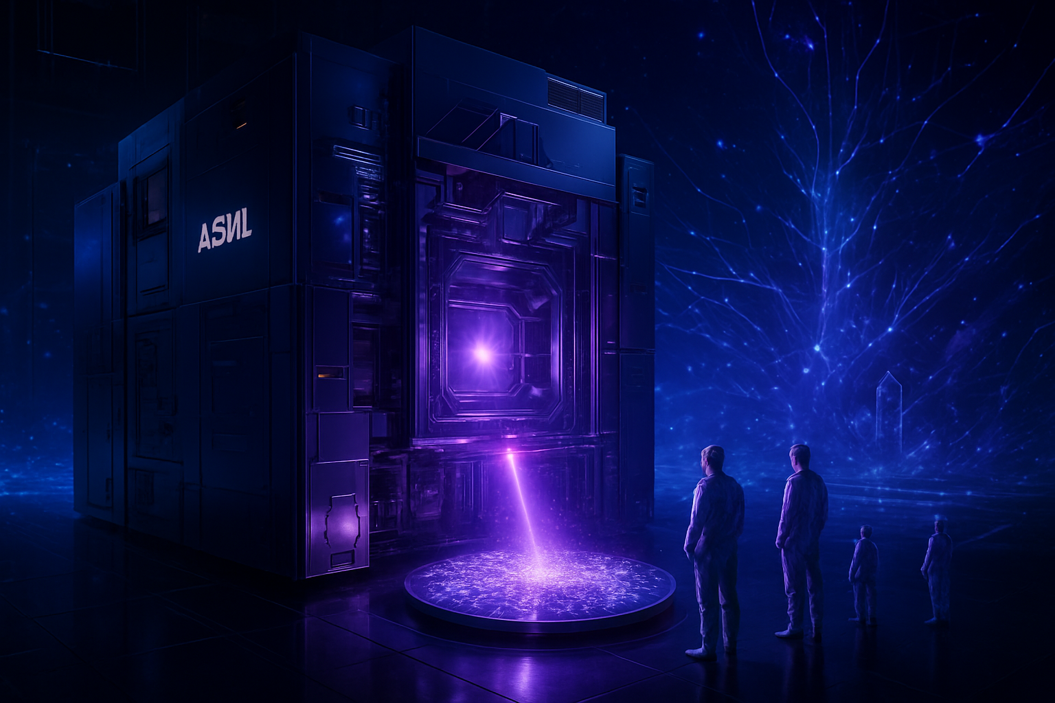
In a landmark shift for the global semiconductor industry, NVIDIA (NASDAQ: NVDA) and TSMC (NYSE: TSM) have officially commenced high-volume production of the "Blackwell" AI architecture at TSMC’s Fab 21 in North Phoenix, Arizona. As of February 5, 2026, the facility has reached yield parity with TSMC’s flagship plants in Taiwan, silencing skeptics who questioned whether advanced chip manufacturing could be successfully replicated in the United States. This development marks the first time in decades that the world’s most sophisticated silicon—the literal engine of the generative AI revolution—is being fabricated domestically.
The achievement represents more than just a logistical win; it is a geopolitical insurance policy for the American AI infrastructure. For years, the concentration of 4nm and 3nm production in the Taiwan Strait was viewed as a "single point of failure" for the global economy. By successfully transitioning the Blackwell B200 and B100 GPUs to Arizona soil, NVIDIA and TSMC have provided a strategic buffer for U.S.-based cloud providers and government agencies, ensuring that the supply of the world's most powerful AI chips remains stable even amidst rising international tensions.
Inside the Arizona Fab: The Technical Feat of 'Yield Parity'
The successful ramp-up at Fab 21 Phase 1 is a technical masterclass in process replication. The Blackwell chips are manufactured using TSMC’s custom 4NP process, a performance-tuned variant of the 5nm (N5) family specifically optimized for the staggering 208 billion transistors found on a single Blackwell GPU. While the "first wafer" was ceremonially signed by NVIDIA CEO Jensen Huang and TSMC executives in October 2025, the real breakthrough occurred in late January 2026, when internal audits confirmed that silicon yields—the percentage of functional chips per wafer—had reached the high-80% to low-90% range, matching the efficiency of TSMC’s primary Tainan facilities.
This technical achievement is significant because advanced chip manufacturing is notoriously sensitive to local environmental factors, including water purity, vibration, and labor expertise. To bridge the gap, TSMC deployed a "copy-exactly" strategy, rotating thousands of American engineers through its Taiwan headquarters while flying in specialized technicians to Phoenix. Industry experts note that Blackwell’s dual-die design, which connects two high-performance chips via a 10 TB/s interconnect, leaves almost no margin for error during the lithography process. Reaching parity on such a complex architecture is a validation of the "reindustrialization" of the American desert.
However, a critical technical nuance remains: the "Taiwan Loop." While the silicon wafers are now fabricated in Arizona, they must still be shipped back to Taiwan for CoWoS (Chip-on-Wafer-on-Substrate) advanced packaging. This final step, where the GPU is bonded to High Bandwidth Memory (HBM3e), is currently the primary bottleneck in the AI supply chain. Although TSMC has announced plans to bring advanced packaging to Arizona through a partnership with Amkor Technology (NASDAQ: AMKR), that domestic loop is not expected to be fully closed until late 2027.
Hyperscale Hunger: How 'Made in USA' Reshapes the AI Market
The shift to domestic production has immediate strategic implications for the "Magnificent Seven" tech giants. Microsoft (NASDAQ: MSFT), Alphabet (NASDAQ: GOOGL), and Meta Platforms (NASDAQ: META) have collectively pledged over $400 billion in capital expenditures for 2026, much of which is earmarked for Blackwell clusters. The availability of U.S.-fabricated chips allows these companies to claim a more secure and ethically "onshored" supply chain, which is becoming a requirement for high-level government and defense AI contracts.
Despite this supply-side victory, the market remains volatile. As of early February 2026, NVIDIA’s stock has faced a "reality check" repricing, falling to a year-to-date low of approximately $172 per share. This dip is attributed to broader sector contagion—led by a weak earnings guide from rival AMD (NASDAQ: AMD)—and emerging concerns that the massive infrastructure spend by cloud providers may take longer to yield a return on investment (ROI). Furthermore, a recent report in the Financial Times alleging that specific NVIDIA optimizations were utilized by the Chinese firm DeepSeek has sparked fears of even tighter export controls, potentially complicating the global distribution of these Arizona-made chips.
For startups and mid-tier AI labs, the Arizona facility provides a glimmer of hope for shorter lead times. Previously, the wait for Blackwell H100 or B200 units could exceed 52 weeks. With Fab 21 now in high-volume mode, analysts predict that wait times could stabilize to under 20 weeks by mid-2026, lowering the barrier to entry for smaller companies attempting to train frontier-class models.
The CHIPS Act Legacy and the Future of Sovereign AI
The success of the Blackwell Arizona rollout is being hailed as the ultimate validation of the CHIPS and Science Act. TSMC’s Arizona project, supported by $6.6 billion in direct federal grants and over $5 billion in loans, was long criticized as a potential "white elephant." Today, it stands as the cornerstone of America's sovereign AI strategy. By de-risking the fabrication process, the U.S. has effectively decoupled the production of its most vital technology from the immediate geographical risks of the Pacific.
In comparison to previous milestones, such as the initial 5nm transition in 2020, the Arizona Blackwell ramp-up is a different kind of breakthrough. It is not about a new process node—the 4NP technology is well-understood—but about the mobility of advanced manufacturing. The ability to move a "cutting-edge" process across the ocean and maintain yield parity within two years suggests that the global semiconductor map is being redrawn. This move toward "technological regionalism" is likely to be emulated by the European Union and Japan as they seek to build their own sovereign AI stacks.
However, concerns persist regarding the "dilution of margins." TSMC has guided for a 3–4% gross margin impact in 2026 due to the higher operating costs of U.S. fabs, including labor, energy, and environmental compliance. Whether the market is willing to pay a "security premium" for U.S.-made chips remains to be seen, but for now, the strategic value appears to outweigh the operational overhead.
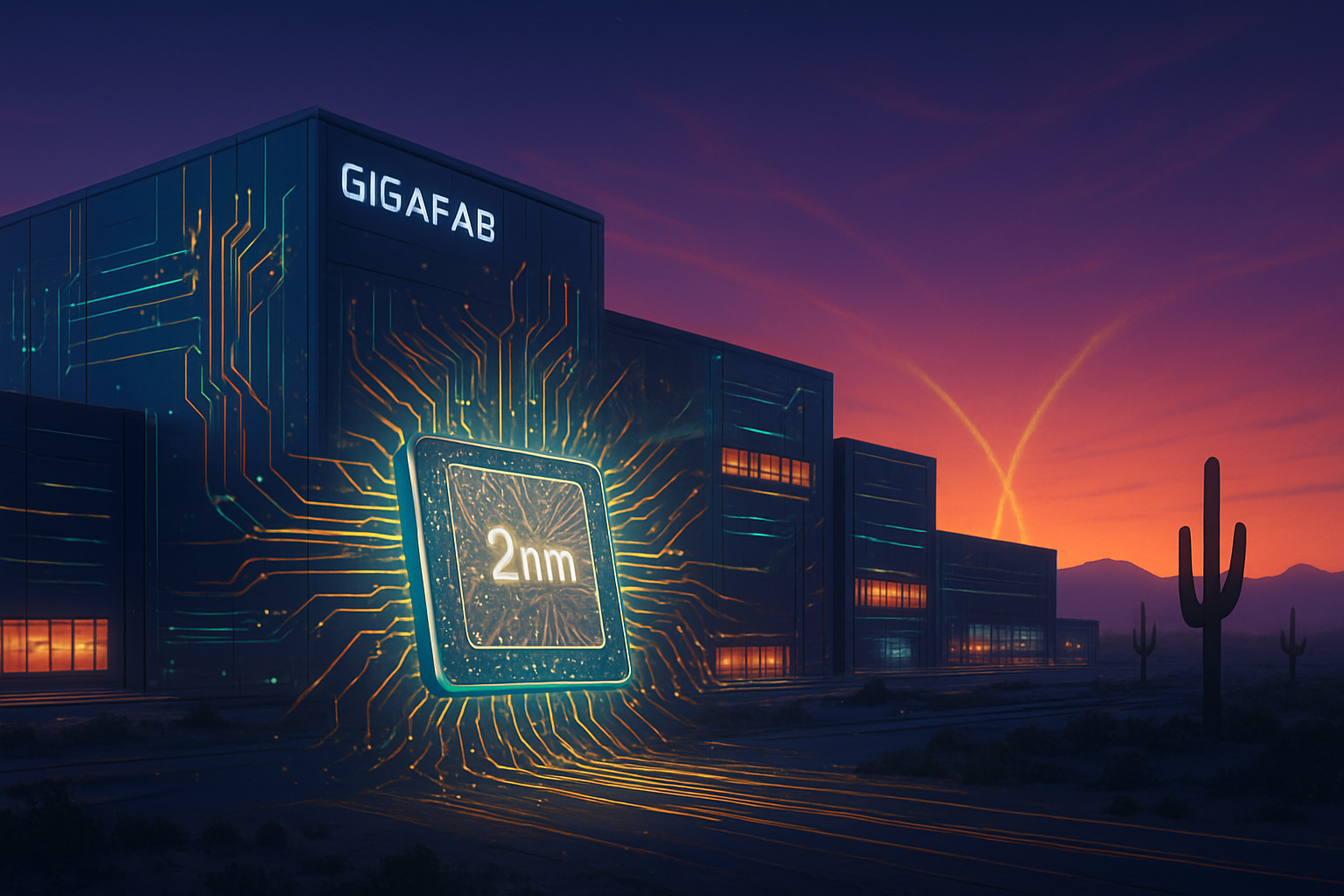
The Road to 2nm: What's Next for the Phoenix Cluster?
The Blackwell milestone is only the beginning for the Arizona "Silicon Desert." On January 15, 2026, TSMC Chairman C.C. Wei announced that the schedule for the second Arizona fab has been accelerated. This second facility is slated to produce 2nm (N2) technology—the next generation of silicon—with equipment installation expected to begin in late 2026 and mass production in 2027. This acceleration is a direct response to the insatiable demand for even more efficient AI training hardware.
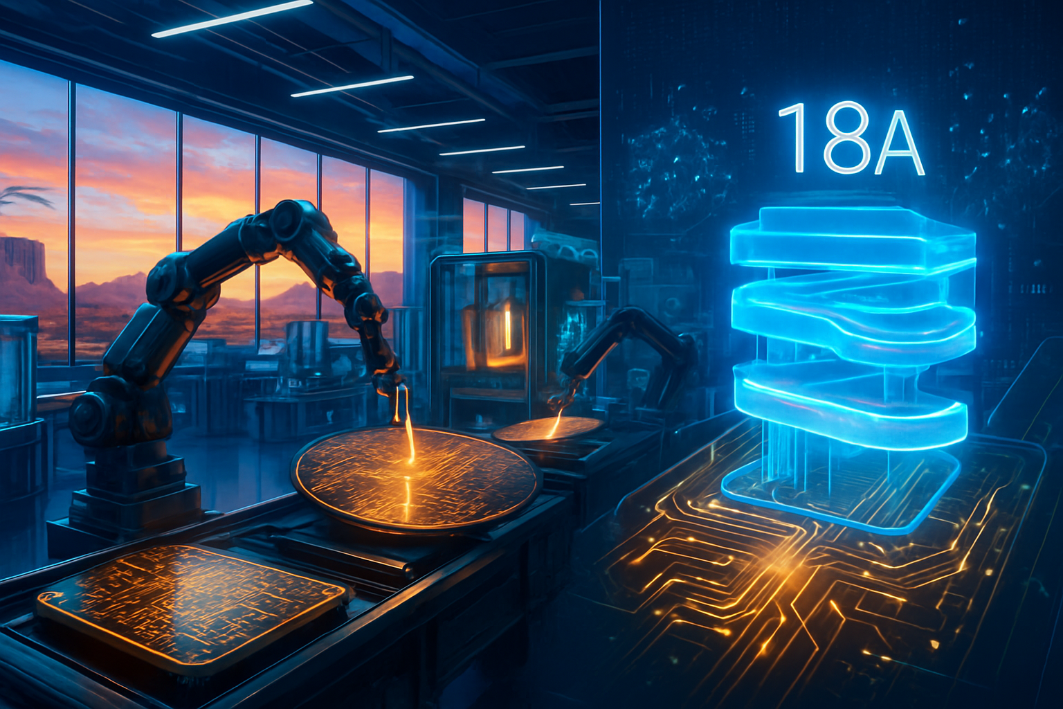
Looking forward, the industry is watching for the emergence of the "Rubin" architecture, NVIDIA’s successor to Blackwell. While Blackwell currently dominates the conversation, rumors from supply chain insiders suggest that the first Rubin test wafers could appear in Arizona as early as 2027. The ultimate goal is a fully vertical U.S. supply chain where the silicon is fabricated, packaged, and assembled into server racks without ever leaving the North American continent.
The primary challenge remaining is the workforce. While yield parity has been achieved, maintaining it at the 2nm scale will require an even more specialized labor pool. The ongoing collaboration between TSMC, the U.S. government, and local universities will be the deciding factor in whether Phoenix becomes a permanent global hub or remains a subsidized outpost of the Taiwanese ecosystem.
A New Chapter in the History of Computing
The successful production of Blackwell wafers in Arizona is a watershed moment in the history of computing. It marks the end of the "Offshore Era," where the world’s most advanced hardware was exclusively the product of a fragile, globalized supply chain. As of February 2026, the United States has reclaimed a seat at the table of leading-edge manufacturing, ensuring that the foundational layers of the AI era are built on stable ground.
The key takeaway for investors and industry watchers is that the "AI bottleneck" has officially shifted. It is no longer a question of whether the world can make enough chips, but whether the software and energy infrastructure can keep up with the sheer volume of silicon now flowing out of both Taiwan and Arizona. In the coming months, all eyes will be on the Amkor packaging facility and the progress of Fab 21’s Phase 2, as the U.S. attempts to finish the job it started with the CHIPS Act.
For now, the signed Blackwell wafer sitting in TSMC’s Phoenix headquarters serves as a powerful symbol: the future of AI is no longer just "Designed in California"—it is increasingly "Made in Arizona."
This content is intended for informational purposes only and represents analysis of current AI developments.
TokenRing AI delivers enterprise-grade solutions for multi-agent AI workflow orchestration, AI-powered development tools, and seamless remote collaboration platforms.
For more information, visit https://www.tokenring.ai/.