Tag: TSMC

  • NVIDIA Overtakes Apple as TSMC’s Top Customer: The Dawn of the AI Utility Phase

    NVIDIA Overtakes Apple as TSMC’s Top Customer: The Dawn of the AI Utility Phase

    In a watershed moment for the global semiconductor industry, NVIDIA (NASDAQ: NVDA) has officially surpassed Apple (NASDAQ: AAPL) to become the largest revenue contributor for Taiwan Semiconductor Manufacturing Company (TSMC) (NYSE: TSM). Financial data emerging in early 2026 reveals a tectonic shift in the foundry’s client hierarchy: NVIDIA is projected to generate approximately $33 billion in revenue for TSMC this year, accounting for 22% of the total, while Apple, the long-standing "alpha" customer, is expected to contribute $27 billion, or roughly 18%.

    This reversal marks the first time in over a decade that a company other than Apple has held the top spot at the world’s premier chipmaker. The development is more than just a corporate milestone; it signals a fundamental realignment of the global economy. For the past fifteen years, the semiconductor market was largely defined by the smartphone and consumer electronics boom led by Apple. Today, that mantle has passed to the builders of artificial intelligence infrastructure, marking the definitive arrival of the "AI era" in industrial manufacturing.

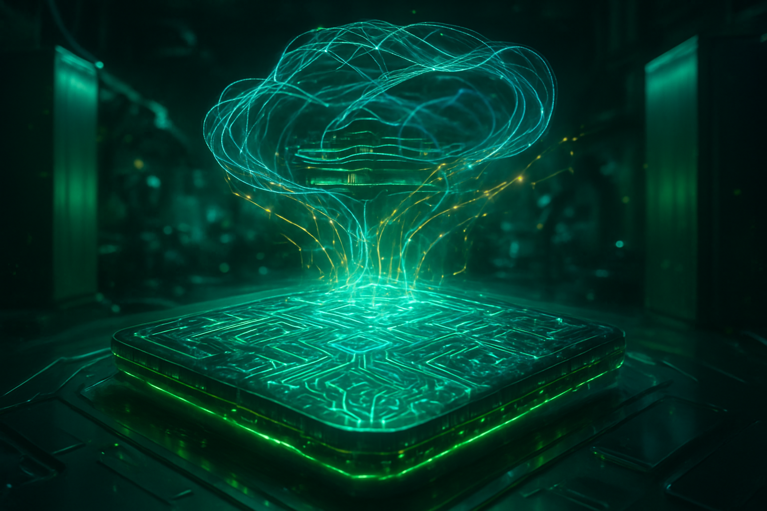
    The Architecture of Dominance: Blackwell, Rubin, and the CoWoS Bottleneck

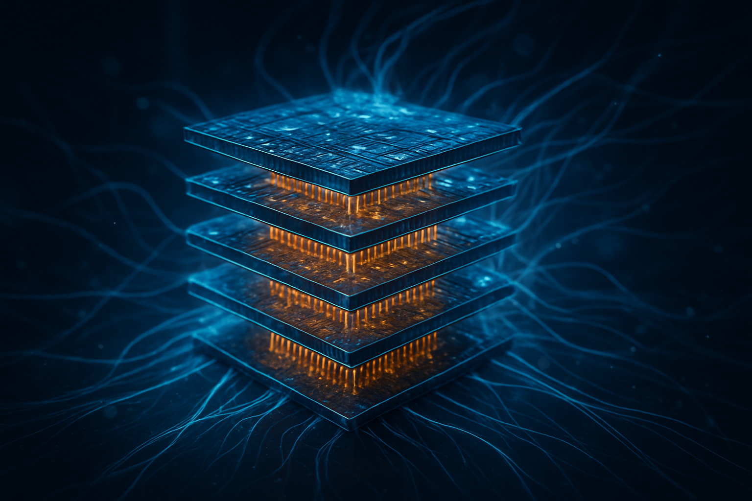
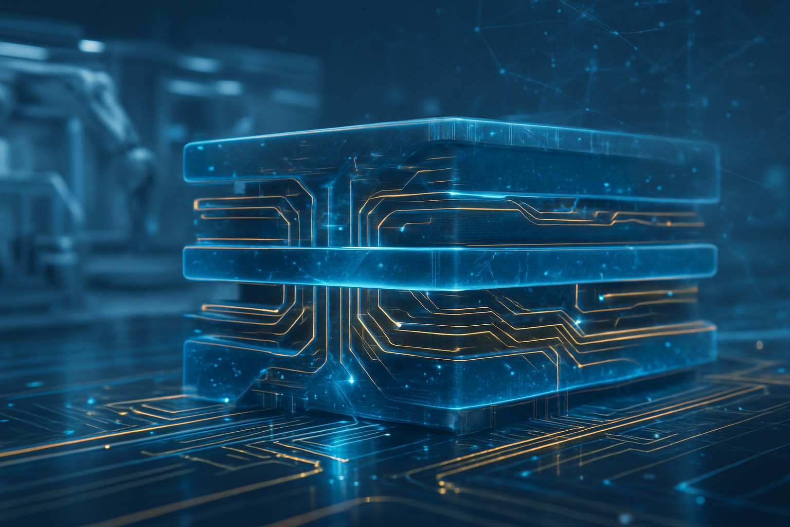
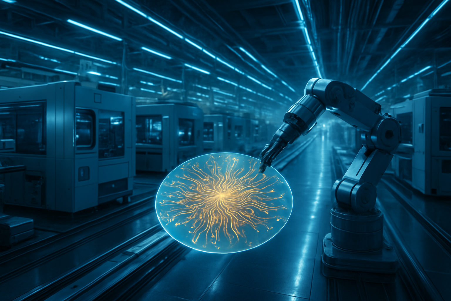
    The primary catalyst for this revenue surge is the sheer physical and technical complexity of NVIDIA’s latest silicon architectures. Unlike consumer-grade chips found in iPhones or MacBooks, which are optimized for power efficiency and mass-market costs, NVIDIA’s high-end AI accelerators like the Blackwell Ultra (GB300) and the upcoming Vera Rubin (R100) platforms are massive, high-performance systems. These chips push the boundaries of "reticle size"—the maximum area a single chip can occupy on a wafer—often requiring multiple dies to be stitched together with extreme precision. This complexity allows TSMC to command significantly higher prices per wafer compared to the smaller, more streamlined A-series chips produced for Apple.

    A critical component of this revenue growth is TSMC’s Chip on Wafer on Substrate (CoWoS) packaging technology. As AI models demand faster data throughput, the "glue" that connects GPUs with High-Bandwidth Memory (HBM) has become the industry’s most valuable bottleneck. NVIDIA has reportedly secured nearly 60% of TSMC’s entire CoWoS capacity for 2026. This advanced packaging is a high-margin service that adds a substantial layer of revenue on top of traditional wafer fabrication. By late 2026, TSMC’s CoWoS capacity is expected to reach over 100,000 wafers per month to keep pace with NVIDIA’s relentless release cycle.

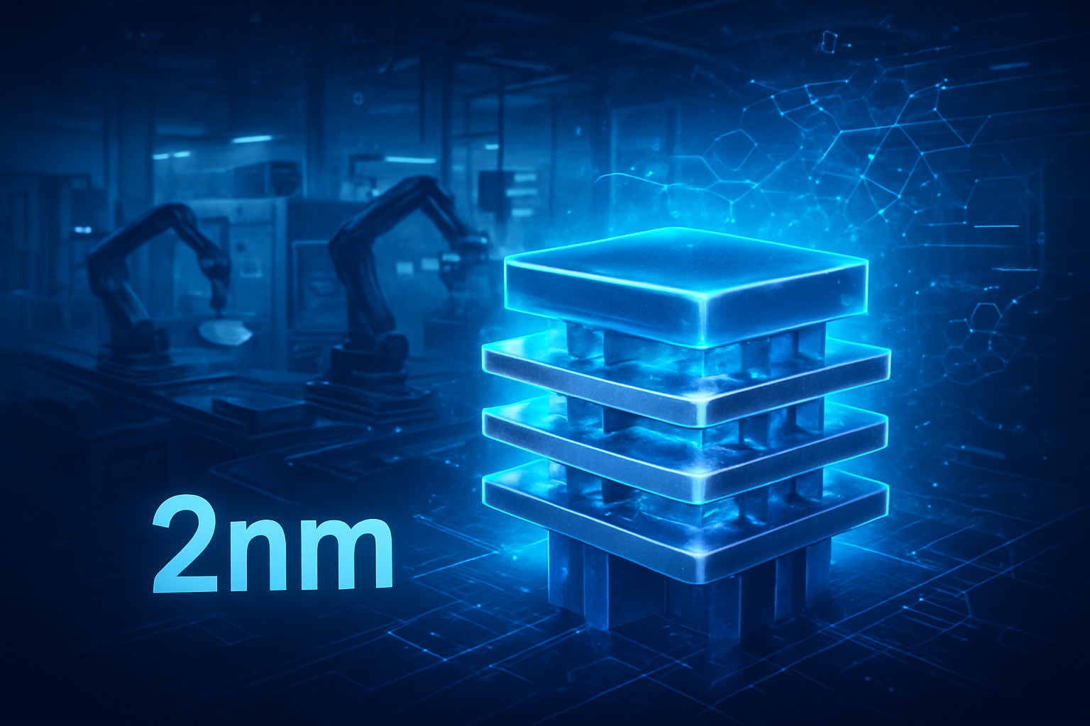
    Initial reactions from the semiconductor research community suggest that NVIDIA’s move to the top spot was inevitable given the massive die sizes of the Rubin architecture. Analysts note that while Apple still ships hundreds of millions more individual chips than NVIDIA, the "value-per-wafer" for an AI accelerator is orders of magnitude higher. Industry experts believe this creates a "priority lock" where NVIDIA now gets first access to TSMC's most advanced nodes, such as the upcoming 2nm (N2) process, a privilege previously reserved almost exclusively for Apple.

    Reshaping the Tech Titan Hierarchy

    This shift has profound implications for the competitive landscape of Big Tech. For years, Apple’s dominance at TSMC gave it a strategic "moat," ensuring its products had the most efficient processors on the market before anyone else. Now, with NVIDIA as the primary revenue driver, TSMC is increasingly incentivized to prioritize the high-performance computing (HPC) requirements of AI over the low-power requirements of mobile devices. This could potentially slow the pace of performance gains in consumer hardware while accelerating the capabilities of the data centers that power AI services.

    Major AI labs and cloud providers—including Microsoft (NASDAQ: MSFT), Amazon (NASDAQ: AMZN), and Alphabet (NASDAQ: GOOGL)—stand to benefit from this alignment, as NVIDIA’s primary status ensures a steady, albeit expensive, supply of the hardware needed to scale their generative AI products. However, the high cost of NVIDIA’s Rubin platform, which targets a 10x reduction in token generation costs, creates a high barrier to entry for smaller startups. These companies must now navigate a market where the "silicon tax" is increasingly paid to a single, dominant provider that sits at the top of the manufacturing food chain.

    The strategic advantage has clearly pivoted. NVIDIA's ability to command TSMC’s roadmap means the foundry is now optimizing its future factories for "big silicon" rather than "small silicon." This transition forces competitors like AMD (NASDAQ: AMD) to compete for the remaining advanced packaging capacity, potentially tightening the supply of rival AI chips and further cementing NVIDIA’s market positioning as the de facto gatekeeper of AI compute.

    Entering the 'Utility Phase' of the AI Cycle

    Market analysts are describing this period as the transition from the "Land Grab Phase" to the "Utility Phase" of the AI cycle. During 2023 and 2024, the industry saw a frantic, speculative rush to acquire any available GPUs to avoid being left behind. In 2026, the focus has shifted toward Return on Investment (ROI) and enterprise-wide productivity. AI is no longer a peripheral experiment; it has become a core utility, as essential to modern business as electricity or high-speed internet.

    The fact that NVIDIA has overtaken Apple—a company built on consumer desire—indicates that the AI cycle is now driven by industrial necessity. This stage of the cycle requires a drastic reduction in the cost of intelligence to remain sustainable. This is why the Rubin architecture is so significant; by focusing on slashing the cost per token, NVIDIA is making it economically viable for businesses to embed AI into every layer of their software stacks. It represents a move toward the commoditization of high-level reasoning.

    Comparatively, this milestone is being likened to the moment in the early 20th century when industrial power generation surpassed residential lighting as the primary driver of the electrical grid. The sheer scale of infrastructure being built suggests that we are move past the "hype" and into a decade-long deployment phase. While concerns about an "AI bubble" persist, the hard capital expenditures flowing from the world’s most valuable companies into TSMC’s foundries suggest a long-term commitment to this technological pivot.

    The Horizon: 2nm and Beyond

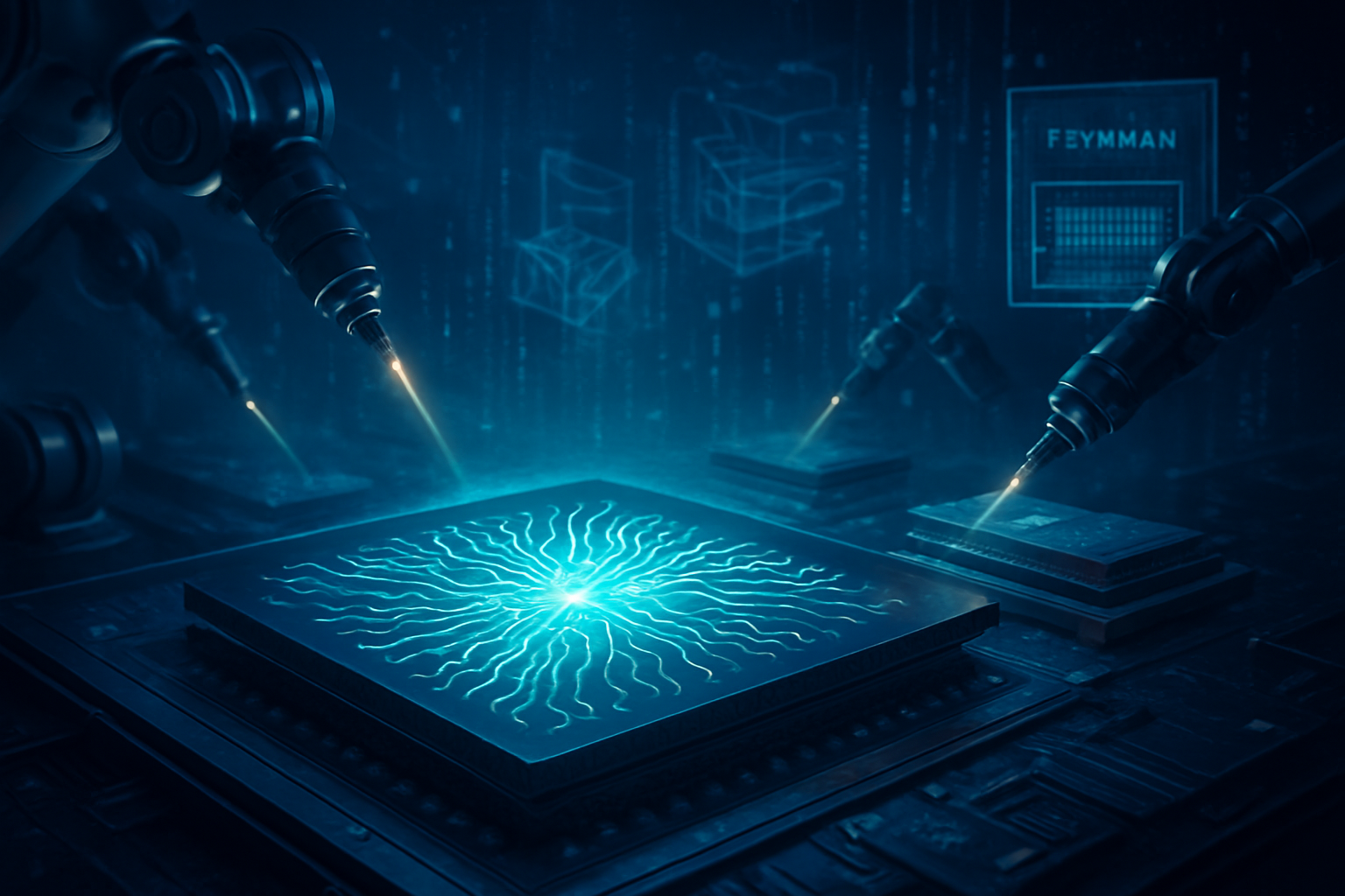
    Looking ahead, the next battleground will be the transition to the 2nm (N2) process node, expected to ramp up in late 2026 and 2027. Experts predict that NVIDIA will be the lead customer for this node, utilizing "GAAFET" (Gate-All-Around Field-Effect Transistor) technology to further increase the density of its Rubin-successor chips. The challenge will not just be fabrication, but the continued scaling of HBM and advanced packaging, which remain prone to yield issues and supply chain disruptions.

    In the near term, we can expect NVIDIA to push deeper into vertical integration, perhaps offering more tailored "AI factories" that include not just the chips, but the liquid cooling and networking stacks required to run them. The goal is to move from selling components to selling entire units of "intelligence." Challenges remain, particularly regarding the massive power consumption of these new data centers and the geopolitical tensions surrounding semiconductor manufacturing in the Taiwan Strait, which remains a singular point of failure for the global AI economy.

    A New Era in Computing History

    The ascension of NVIDIA to the top of TSMC’s customer list is a historic realignment that marks the end of the mobile-first era and the beginning of the AI-first era. It underscores a shift in value from the device in our pockets to the massive, distributed intelligence engines in the cloud. NVIDIA’s $33 billion contribution to TSMC’s coffers is the ultimate proof of the industry's belief in the permanence of the AI revolution.

    As we move through 2026, the key metrics to watch will be the "cost-per-token" metrics provided by the Rubin platform and the speed at which TSMC can expand its CoWoS capacity. If NVIDIA can continue to lower the cost of AI while maintaining its lead at the foundry, it will solidify its role as the foundational utility of the 21st century. The world is no longer just buying gadgets; it is building a new kind of cognitive infrastructure, and for the first time, the numbers at the world's most important factory prove it.


    This content is intended for informational purposes only and represents analysis of current AI developments.

    TokenRing AI delivers enterprise-grade solutions for multi-agent AI workflow orchestration, AI-powered development tools, and seamless remote collaboration platforms.
    For more information, visit https://www.tokenring.ai/.

  • Beyond the Shrink: How 6-Micrometer Hybrid Bonding is Resurrecting Moore’s Law for the AI Era

    Beyond the Shrink: How 6-Micrometer Hybrid Bonding is Resurrecting Moore’s Law for the AI Era

    As of early 2026, the semiconductor industry has reached a definitive turning point where the traditional method of scaling—simply making transistors smaller—is no longer the primary driver of computing power. Instead, the focus has shifted to "Advanced Packaging," a sophisticated method of stacking and connecting multiple chips to act as a single, massive processor. At the heart of this revolution is Taiwan Semiconductor Manufacturing Company (NYSE: TSM), whose System on Integrated Chips (SoIC) technology has become the industry standard for bridging the gap between theoretical chip designs and the massive computational demands of generative AI.

    The move to 6-micrometer (6µm) bond pitches represents the current "Goldilocks" zone of semiconductor manufacturing, providing the density required for next-generation AI accelerators like NVIDIA’s (NASDAQ: NVDA) upcoming Rubin architecture and AMD’s (NASDAQ: AMD) Instinct MI400 series. By utilizing hybrid bonding—a process that replaces traditional solder bumps with direct copper-to-copper connections—manufacturers are successfully bypassing the physical limits of monolithic silicon, effectively keeping Moore’s Law alive through vertical integration rather than horizontal shrinkage.

    The Technical Frontier: SoIC and the 6µm Milestone

    TSMC’s SoIC technology represents the pinnacle of 3D heterogeneous integration, specifically through its "bumpless" hybrid bonding technique known as SoIC-X. Unlike traditional 2.5D packaging, which places chips side-by-side on a silicon interposer (such as CoWoS), SoIC-X allows for logic-on-logic stacking. By reducing the bond pitch—the distance between interconnects—to 6 micrometers, TSMC has achieved a 100x increase in interconnect density compared to the 30-40µm pitches used in traditional micro-bump technologies. This leap allows for massive bandwidth between stacked dies, essentially eliminating the latency that usually occurs when data travels between different parts of a processor.

    Technical specifications for the 2026 roadmap indicate that while 6µm is the current high-volume standard, the industry is already testing 4µm and 3µm pitches for late 2026 deployments. This roadmap is critical for the integration of HBM4 (High Bandwidth Memory), which requires these ultra-fine pitches to manage the thermal and electrical signaling of 16-high memory stacks. Initial reactions from the research community have been overwhelmingly positive, with engineers noting that 6µm hybrid bonding allows them to treat separate chiplets as a single "virtual monolithic" die, granting the architectural freedom to mix and match different process nodes (e.g., a 2nm compute die on a 5nm I/O die).

    Market Dynamics: The Battle for AI Supremacy

    The shift toward high-density hybrid bonding has ignited a fierce competitive landscape among chip designers and foundries. NVIDIA (NASDAQ: NVDA) has pivoted its roadmap to take full advantage of TSMC’s SoIC, moving away from the side-by-side Blackwell designs toward the fully 3D-stacked Rubin platform. This move solidifies NVIDIA’s market positioning by allowing it to pack significantly more compute power into the same physical footprint, a necessity for the power-constrained environments of modern data centers. Meanwhile, AMD (NASDAQ: AMD) continues to leverage its early-mover advantage in 3D stacking; having pioneered SoIC with the MI300, it is now utilizing 6µm bonding in the MI400 to maintain its lead in memory capacity and bandwidth.

    However, TSMC is not the only player in this space. Intel (NASDAQ: INTC) is aggressively pushing its Foveros Direct 3D technology, which aims for sub-5µm pitches to support its 18A-PT process node. Intel’s "Clearwater Forest" Xeon processors are the first major test of this technology, positioning the company as a viable alternative for AI companies looking to diversify their supply chains. Samsung (KRX: 005930) is also a major contender with its X-Cube and SAINT platforms. Samsung's unique strategic advantage lies in its "turnkey" capability: it is currently the only company that can manufacture the HBM memory, the logic dies, and the advanced 3D packaging under one roof, potentially lowering costs for hyperscalers like Google or Meta.

    Wider Significance: A New Paradigm for Moore’s Law

    The wider significance of 6µm hybrid bonding cannot be overstated; it represents the shift from the "Era of Shrink" to the "Era of Integration." For decades, Moore's Law relied on the ability to double transistor density on a single piece of silicon every two years. As that process has become exponentially more expensive and physically difficult, advanced packaging has stepped in as the "Silicon Lego" solution. By stacking chips vertically, designers can continue to increase transistor counts without the catastrophic yield losses associated with building giant, monolithic chips.

    This development also addresses the "memory wall"—the bottleneck where processor speed outpaces the speed at which data can be fetched from memory. 3D stacking places memory directly on top of the logic, reducing the distance data must travel and significantly lowering power consumption. However, this transition brings new concerns, primarily regarding thermal management. Stacking high-performance logic dies creates "heat sandwiches" that require innovative cooling solutions, such as microfluidic cooling or advanced diamond-based thermal spreaders, to prevent the chips from throttling or failing.

    The Horizon: Glass Substrates and Sub-3µm Pitches

    Looking ahead, the industry is already identifying the next hurdles beyond 6µm bonding. The next two to three years will likely see the adoption of glass substrates to replace traditional organic materials. Glass offers superior flatness and thermal stability, which is essential as bond pitches continue to shrink toward 2µm and 1µm. Experts predict that by 2028, we will see the first "3.5D" architectures in the wild—complex systems where multiple 3D-stacked logic towers are interconnected on a glass interposer, providing a level of complexity that was unimaginable a decade ago.

    The challenges remaining are primarily economic and logistical. The equipment required for hybrid bonding, such as high-precision wafer-to-wafer aligners, is currently in short supply, and the "cleanliness" requirements for a 6µm bond are far stricter than for traditional packaging. Any microscopic dust particle can ruin a hybrid bond, leading to lower yields. As the industry moves toward these finer pitches, the role of automated inspection and AI-driven quality control will become just as important as the bonding technology itself.

    Conclusion: The 3D Future of Artificial Intelligence

    The transition to 6-micrometer hybrid bonding and TSMC’s SoIC platform marks a definitive end to the "monolithic era" of computing. As of January 30, 2026, the success of the world’s most powerful AI models is now inextricably linked to the success of 3D vertical stacking. By allowing for unprecedented interconnect density and bandwidth, advanced packaging has provided the industry with a second wind, ensuring that the computational gains required for the next phase of AI development remain achievable.

    In the coming months, keep a close eye on the production yields of NVIDIA’s Rubin and the initial benchmarks of Intel’s 18A-PT products. These will serve as the litmus test for whether hybrid bonding can be scaled to the volumes required by the insatiable AI market. While the physical limits of the transistor may be in sight, the architectural possibilities of 3D integration are just beginning to be explored. Moore’s Law isn’t dead; it has simply moved into the third dimension.


    This content is intended for informational purposes only and represents analysis of current AI developments.

    TokenRing AI delivers enterprise-grade solutions for multi-agent AI workflow orchestration, AI-powered development tools, and seamless remote collaboration platforms.
    For more information, visit https://www.tokenring.ai/.

  • Silicon’s New Horizon: TSMC Hits 2nm Milestone as GAA Transition Reshapes AI Hardware

    Silicon’s New Horizon: TSMC Hits 2nm Milestone as GAA Transition Reshapes AI Hardware

    As of January 30, 2026, the global semiconductor landscape has officially entered the "Angstrom Era." Taiwan Semiconductor Manufacturing Company (NYSE: TSM), the world's largest contract chipmaker, has successfully transitioned its 2nm (N2) process from pilot lines to high-volume manufacturing (HVM). This milestone represents more than just a reduction in feature size; it marks the most significant architectural overhaul in semiconductor design since the introduction of FinFET over a decade ago.

    The immediate significance of the N2 node cannot be overstated, particularly for the burgeoning artificial intelligence sector. With production now scaling at TSMC's Baoshan and Kaohsiung facilities, the first wave of 2nm-powered devices is expected to hit the market by the end of the year. This shift provides the critical hardware foundation required to sustain the massive compute demands of next-generation large language models and autonomous systems, effectively extending the lifespan of Moore’s Law through sheer architectural ingenuity.

    The Nanosheet Revolution: Engineering the 2nm Breakthrough

    The technical centerpiece of the N2 node is the transition from the long-standing FinFET (Fin Field-Effect Transistor) architecture to Gate-All-Around (GAA) technology, which TSMC refers to as "Nanosheet" transistors. In previous FinFET designs, the gate covered three sides of the channel. However, as transistors shrunk toward the 2nm limit, electron leakage became an insurmountable hurdle. The Nanosheet design solves this by wrapping the gate entirely around the channel on all four sides. This provides superior electrostatic control, virtually eliminating current leakage and allowing for significantly lower operating voltages.

    Beyond the transistor geometry, TSMC has introduced a proprietary feature known as NanoFlex™. This technology allows chip designers at firms like Apple (NASDAQ: AAPL) and NVIDIA (NASDAQ: NVDA) to mix and match different standard cell types—short cells for power efficiency and tall cells for peak performance—on a single die. This granular control over the power-performance-area (PPA) profile is unprecedented. Early reports from January 2026 indicate that TSMC has achieved logic test chip yields between 70% and 80%, a remarkable feat that places them well ahead of competitors like Samsung (KRX: 005930), whose 2nm GAA yields are reportedly struggling in the 40-55% range.

    In terms of raw performance, the N2 process is delivering a 10% to 15% speed increase at the same power level compared to the refined 3nm (N3E) process. Perhaps more importantly for mobile and edge AI applications, it offers a 25% to 30% reduction in power consumption at the same clock speed. This efficiency gain is the primary driver for the massive industry interest, as it allows for more complex AI processing to occur on-device without devastating battery life or thermal envelopes.

    The 2026 Capacity Crunch: Apple and NVIDIA Lead the Charge

    The scramble for 2nm capacity has created a "supply choke" that has defined the early months of 2026. Industry insiders confirm that TSMC’s N2 capacity is effectively fully booked through the end of the year, with Apple and NVIDIA emerging as the dominant stakeholders. Apple has reportedly secured over 50% of the initial 2nm output, which it plans to utilize for its upcoming A20 Bionic chips in the iPhone 18 series and the M6 series processors for its MacBook Pro and iPad Pro lineups. For Apple, this exclusivity ensures that its "Apple Intelligence" ecosystem remains the gold standard for on-device AI performance.

    NVIDIA has also made an aggressive play for 2nm wafers to power its "Rubin" GPU platform. As generative AI workloads continue to grow exponentially, NVIDIA’s move to 2nm is seen as a strategic necessity to maintain its dominance in the data center. By moving to the N2 node, NVIDIA can pack more CUDA cores and specialized AI accelerators into a single chip while staying within the power limits of modern liquid-cooled server racks. This has placed smaller AI startups and rival chipmakers in a precarious position, as they must compete for the remaining "leftover" capacity or wait for the 2nm ramp-up to reach 140,000 wafers per month by late 2026.

    The cost of this technological edge is steep. Wafers for the 2nm process are currently estimated at $30,000 each, a 20% premium over the 3nm generation. This pricing reinforces a "winners-take-all" market dynamic, where only the wealthiest tech giants can afford the most advanced silicon. For consumers, this likely translates to higher price points for flagship hardware, but for the industry, it represents the massive capital expenditure required to keep the AI revolution moving forward.

    Redefining the AI Landscape: Sustainability and Sovereignty

    The shift to 2nm has implications that reach far beyond faster smartphones. In the broader AI landscape, the improved power efficiency of N2 is a critical component of the industry’s "green AI" initiatives. As data centers consume an ever-increasing percentage of global electricity, the 30% power reduction offered by 2nm chips becomes a vital tool for sustainability. This allows major cloud providers to expand their AI training clusters without requiring a linear increase in energy infrastructure, mitigating some of the environmental concerns surrounding the AI boom.

    Furthermore, the 2nm milestone solidifies TSMC’s role as the indispensable lynchpin of the global digital economy. As the only foundry currently capable of delivering high-yield 2nm GAA wafers at scale, TSMC’s technological lead has become a matter of national and corporate sovereignty. This has intensified the competitive pressure on Intel (NASDAQ: INTC) and Samsung to accelerate their own roadmaps. While Intel’s 18A process is beginning to gain traction, TSMC’s successful N2 rollout in early 2026 suggests that the "Taiwan Advantage" remains firmly in place for the foreseeable future.

    However, the concentration of 2nm manufacturing in Taiwan remains a point of strategic anxiety for global markets. Despite TSMC’s expansion into Arizona and Japan, the most advanced 2nm "GigaFabs" are currently concentrated in Hsinchu and Kaohsiung. This geopolitical reality means that any disruption in the region would immediately halt the production of the world’s most advanced AI and consumer chips, a vulnerability that continues to drive investments in domestic chip manufacturing in the U.S. and Europe.

    The Road to 1.6nm: Super PowerRail and the A16 Era

    Even as N2 production ramps up, TSMC is already looking toward its next major leap: the A16 (1.6nm) node. Scheduled for high-volume manufacturing in the second half of 2026, A16 will introduce "Super PowerRail" (SPR) technology. This is TSMC’s proprietary implementation of a Backside Power Delivery Network (BSPDN). Traditionally, power and signal lines are bundled on the front side of a wafer. SPR moves the power delivery to the back, connecting it directly to the transistor's source and drain.

    This innovation is expected to free up nearly 20% more space for signal routing on the front side, significantly reducing "IR drop" (voltage loss) and improving power delivery efficiency. Experts predict that A16 will provide an additional 8% to 10% speed boost over N2P (the performance-enhanced version of 2nm). However, moving the power network to the backside presents a new set of thermal management challenges, as the chip's ability to spread heat laterally is reduced. This will likely necessitate new cooling solutions, such as microfluidic channels integrated directly into the chip packaging.

    Looking ahead, the successful deployment of Super PowerRail in the A16 process will be the defining technical challenge of 2027. If TSMC can solve the thermal hurdles associated with backside power, it will pave the way for chips that are not only smaller but fundamentally more efficient at handling the high-intensity, continuous compute required for real-time AI reasoning and 8K holographic rendering.

    Conclusion: A New Era of Silicon Dominance

    TSMC’s 2nm production milestone is a watershed moment in the history of computing. By successfully navigating the transition from FinFET to Nanosheet architecture, the company has provided the world’s leading technology companies with the tools needed to push AI beyond current limitations. The fact that 2026 capacity is already spoken for by Apple and NVIDIA underscores the desperate industry-wide need for more efficient, more powerful silicon.

    As we move through the first quarter of 2026, the key metrics to watch will be the continued stabilization of N2 yields and the first real-world benchmarks from 2nm-equipped devices. While the A16 roadmap and Super PowerRail technology promise even greater gains, the current focus remains on the flawless execution of N2. For the AI industry, the message is clear: the hardware bottleneck is widening, but the price of entry into the elite tier of performance has never been higher. TSMC's achievement ensures that the momentum of the AI era continues unabated, firmly establishing the 2nm node as the backbone of the next generation of digital innovation.


    This content is intended for informational purposes only and represents analysis of current AI developments.

    TokenRing AI delivers enterprise-grade solutions for multi-agent AI workflow orchestration, AI-powered development tools, and seamless remote collaboration platforms.
    For more information, visit https://www.tokenring.ai/.

  • Apple’s Silicon Fortress: Securing 2nm Hegemony and the Impending Yield Generation Gap

    Apple’s Silicon Fortress: Securing 2nm Hegemony and the Impending Yield Generation Gap

    As the semiconductor industry hurtles toward the "Angstrom Era," Apple Inc. (NASDAQ: AAPL) has reportedly moved to solidify a total technological monopoly for 2026. Industry insiders and supply chain reports confirm that the Cupertino giant has successfully reserved over 50% of Taiwan Semiconductor Manufacturing Company’s (NYSE: TSM) initial 2nm—or N2—manufacturing capacity. By making massive capital prepayments and partnering on a dedicated production facility at TSMC’s Chiayi P1 plant, Apple is effectively "starving" its competitors, ensuring that its upcoming A20 chips will be the first and most widely available processors to utilize the revolutionary Nanosheet architecture.

    This aggressive procurement strategy does more than just secure inventory; it creates a "yield generation gap" that leaves Android competitors in a precarious position. As of late January 2026, TSMC’s 2nm yields have stabilized between 70% and 80%, a milestone that allows Apple to confidently plan a massive September launch for the iPhone 18 Pro. Meanwhile, rivals like Qualcomm (NASDAQ: QCOM) and MediaTek (TPE: 2454) are left to navigate a fractured landscape, forced to either bid for the remaining scraps of TSMC’s high-cost capacity or gamble on Samsung Electronics (KRX: 005930), whose 2nm yields are rumored to be struggling significantly lower.

    The Architecture of Dominance: Nanosheets and the A20

    The shift from the long-standing FinFET (Fin Field-Effect Transistor) architecture to Nanosheet GAAFET (Gate-All-Around) marks the most significant change in transistor design in over a decade. In the N2 process, the gate wraps around all four sides of the channel, providing superior electrostatic control and drastically reducing current leakage. Technical specifications indicate a 10–15% speed increase at the same power level compared to the previous 3nm (N3E) process, or a staggering 25–30% reduction in power consumption at the same clock frequency.

    Central to Apple’s 2026 strategy is the A20 Pro chip, which will debut in the iPhone 18 Pro and the long-rumored "iPhone Fold." Beyond the raw transistor density, the A20 is expected to utilize TSMC’s Wafer-level Multi-Chip Module (WMCM) packaging. This allows Apple to tightly integrate the CPU, GPU, and 12GB of high-speed LPDDR6 RAM on a single wafer-level substrate, eliminating the latency inherent in traditional separate memory packages. Initial reactions from the hardware community suggest that this integration is critical for the next phase of "Apple Intelligence," providing the memory bandwidth required for sophisticated, on-device generative AI models that were previously restricted to cloud environments.

    The Yield Generation Gap: A Trap for Android Rivals

    The competitive implications of Apple’s move are profound, creating what analysts call a "yield generation gap." In semiconductor manufacturing, the ability to produce functional chips consistently—the yield—determines the economic viability of a product. With TSMC reporting 75%+ yields on N2, Apple can absorb the projected $30,000-per-wafer cost because its high-margin Pro models can sustain the expense. Apple’s supply chain hegemony ensures that even if a rival has a superior chip design on paper, they may lack the volume to bring it to market at a competitive price point.

    Qualcomm and MediaTek find themselves caught in a strategic trap. With Apple occupying the majority of TSMC’s early capacity, these firms must either delay their 2nm transitions or turn to Samsung’s SF2 process. However, industry reports suggest Samsung is currently seeing yields in the 40–50% range for its 2nm node. History has shown that when Qualcomm was forced to use Samsung’s less mature nodes—as with the Snapdragon 8 Gen 1—the resulting chips suffered from overheating and aggressive performance throttling. This creates a two-year window where Apple's silicon could remain unchallenged in both efficiency and peak performance, as Android manufacturers struggle with either supply constraints or inferior manufacturing stability.

    Broadening the AI Landscape: The High Cost of the Angstrom Era

    This development reflects a broader trend toward "Foundry Monopolies," where only the world’s wealthiest tech giants can afford to participate in the most advanced nodes. The $30,000 wafer price for 2nm represents a 50% increase over 3nm, a barrier to entry that is likely to consolidate the high-end smartphone market further. For the wider AI landscape, Apple’s move signals that the battle for AI supremacy has moved from software optimization to raw silicon capability. By securing the most efficient chips, Apple is betting that superior battery life and on-device privacy will be the winning factors in the AI smartphone wars.

    There are, however, concerns regarding this consolidation. As Apple ties itself closer to TSMC, the geopolitical risks associated with semiconductor production in Taiwan remain a point of discussion among market analysts. Furthermore, the rising cost of the A20 chip—estimated at $280 per unit compared to the A19’s $150—suggests that the era of the $1,000 flagship may be coming to an end, replaced by even higher "Ultra" tier pricing. Comparisons are already being made to the 2017 transition to the iPhone X, though the current shift is driven by invisible internal architecture rather than external design changes.

    Future Horizons: Beyond the First 2nm Wave

    Looking ahead, the road to 2027 and beyond involves even more complex iterations of the 2nm process. While Apple has secured the initial N2 capacity, TSMC is already preparing "N2P," which will introduce backside power delivery—a technique that moves the power wiring to the back of the wafer to reduce interference and boost performance further. Experts predict that Apple will once again be the first in line for this refinement, potentially for the A21 chip.

    In the near term, the focus remains on the September 2026 launch window. The challenge for Apple will be managing the "split-node" strategy; rumors suggest that while the iPhone 18 Pro will receive the 2nm A20, the standard iPhone 18 may utilize an enhanced 3nm (N3P) process to manage costs. This would further differentiate the Pro lineup, making the 2nm chip a exclusive status symbol of performance. The industry is also watching to see if Qualcomm will attempt to bypass 2nm entirely and focus on "High-NA EUV" (High Numerical Aperture Extreme Ultraviolet) lithography for a 1.4nm leap in 2028, though such a move would be fraught with technical risk.

    Summary of the Silicon Stalemate

    Apple’s tactical maneuver to secure over half of TSMC’s 2nm capacity for 2026 is a masterclass in supply chain dominance. By locking in the most advanced manufacturing process three years in advance, the company has not only secured its hardware roadmap but has also effectively handicapped its competition. The "yield generation gap" ensures that for the foreseeable future, the most efficient and powerful AI-ready smartphones will likely carry an Apple logo, simply because no one else can manufacture them at scale.

    This development marks a pivotal moment in AI history, where the physical limits of the "Angstrom Era" are becoming the primary battlefield for tech supremacy. In the coming months, the industry will be watching for Qualcomm’s response and Samsung’s potential yield breakthroughs. However, as of January 2026, the silicon landscape is looking increasingly like a one-player game, with Apple holding all the winning cards at the 2nm table.


    This content is intended for informational purposes only and represents analysis of current AI developments.

    TokenRing AI delivers enterprise-grade solutions for multi-agent AI workflow orchestration, AI-powered development tools, and seamless remote collaboration platforms.
    For more information, visit https://www.tokenring.ai/.

  • Samsung Hits 70% Yield on 2nm GAA (SF2P): A Turning Point for the AI Chip Supply Chain

    Samsung Hits 70% Yield on 2nm GAA (SF2P): A Turning Point for the AI Chip Supply Chain

    As of January 30, 2026, the global semiconductor landscape is undergoing a tectonic shift. Samsung Electronics (KRX: 005930) has officially reached a critical performance and yield milestone for its 2nm (SF2P) production process, signaling a major challenge to the long-standing dominance of Taiwan Semiconductor Manufacturing Company (NYSE: TSM). Following its Q4 2025 earnings report, Samsung confirmed that its performance-optimized 2nm node, known as SF2P, has successfully hit the 70% yield threshold required for stable mass production—a feat that many industry skeptics thought would take years to master.

    This development is more than just a technical victory; it is a strategic lifeline for the world’s largest chip designers. With TSMC’s 2nm capacity currently overwhelmed by exclusive orders from high-priority clients, the emergence of a viable, high-yield alternative from Samsung provides a release valve for a supply chain that has been dangerously bottlenecked. By mastering the intricate Gate-All-Around (GAA) architecture ahead of its rivals, Samsung is positioning itself as the primary destination for the next generation of high-performance AI and mobile processors.

    Engineering the Future: The Maturity of 3rd-Gen GAA

    The SF2P node represents the second generation of Samsung’s 2nm platform, specifically optimized for high-performance computing (HPC) and premium mobile devices. Unlike traditional FinFET transistors, which hit physical scaling limits years ago, Samsung’s 2nm utilizes its proprietary Multi-Bridge Channel FET (MBCFET) architecture—a 3rd-generation evolution of GAA technology. This approach allows for a "nanosheet" design where the width of the channel can be adjusted to optimize for either extreme power efficiency or maximum performance. Compared to the first-generation SF2 node, the 2026-era SF2P delivers a 12% boost in clock speeds, a 25% improvement in power efficiency, and an 8% reduction in total die area.

    Technical experts note that Samsung’s early gamble on GAA—which it first introduced at the 3nm node while TSMC stuck with FinFET—is finally paying dividends. While competitors are only now navigating the "learning curve" of nanosheet production, Samsung has accumulated four years of telemetry data on GAA manufacturing. This experience has allowed the foundry to refine its extreme ultraviolet (EUV) lithography processes and address the "stochastic" defects that typically plague sub-3nm nodes. The result is a more uniform transistor structure that significantly reduces leakage current, a critical requirement for the power-hungry AI workloads of 2026.

    A Strategic Pivot: Qualcomm and AMD Secure Capacity

    The immediate beneficiaries of Samsung’s yield breakthrough are Qualcomm (NASDAQ: QCOM) and AMD (NASDAQ: AMD). As of late January 2026, both companies are reportedly in final negotiations to shift significant portions of their 2nm roadmap to Samsung Foundry. The move is driven by a stark reality: TSMC’s 2nm (N2) capacity is nearly 50% reserved by a single customer, leaving other tech giants fighting for leftovers and paying a "wafer premium" that has risen 50% over previous generations. Qualcomm is expected to utilize SF2P for its next-generation Snapdragon series, while AMD is eyeing the node for its "Venice" EPYC server CPUs to ensure supply stability in the face of skyrocketing enterprise demand.

    This shift represents a significant competitive disruption. For years, TSMC’s "foundry-only" model gave it a reputation for neutrality and reliability that Samsung, a conglomerate that also makes its own consumer products, struggled to match. However, the sheer scale of the AI boom has forced a "dual-sourcing" strategy among major chip designers. By offering competitive yields and more favorable pricing than TSMC, Samsung is transforming the foundry market from a monopoly into a true duopoly. Furthermore, Samsung’s massive $16.5 billion contract with Tesla (NASDAQ: TSLA) for its AI6 autonomous driving chips has served as a powerful "seal of approval," encouraging other automotive and data center players to reconsider their reliance on a single supplier.

    The "One-Stop" AI Solution and the Taylor, Texas Factor

    Samsung’s 2nm success is part of a broader "total solution" strategy that integrates logic, memory, and packaging. In January 2026, Samsung began large-scale shipments of its 12-layer HBM4 (High Bandwidth Memory), a key component for AI accelerators used by NVIDIA (NASDAQ: NVDA) and others. By offering 2nm logic manufacturing alongside HBM4 and advanced X-Cube 3D packaging, Samsung provides a vertically integrated stack that reduces latency and power consumption. This "one-stop shop" capability is something neither TSMC nor Intel (NASDAQ: INTC) can currently match with the same level of internal synchronization, making Samsung an attractive partner for startups building custom "Agentic AI" silicon.

    The geopolitical dimension of this ramp-up cannot be ignored. Samsung’s Taylor, Texas facility is now 93% complete and is transitioning to a "2nm-first" factory. With trial runs of ASML EUV lithography tools scheduled for March 2026, the Taylor fab is set to become a cornerstone of the "Made in USA" advanced chip initiative. This domestic capacity is a major selling point for U.S.-based companies like AMD and Google, who are under increasing pressure to diversify their manufacturing away from the geopolitical sensitivities of the Taiwan Strait. Samsung’s ability to hit 70% yield in its Korean facilities provides the blueprint for a rapid and successful ramp in the United States.

    Looking Ahead: The Road to 1.4nm and Backside Power

    While the industry focuses on the SF2P ramp, Samsung’s R&D teams are already moving toward the next frontier. Near-term developments include the introduction of SF2Z in 2027, which will incorporate Backside Power Delivery Network (BSPDN) technology. This innovation moves the power circuitry to the back of the wafer, freeing up the top side for more transistors and further reducing voltage drops. Beyond 2nm, the roadmap points toward the 1.4nm (SF1.4) node, where Samsung expects to apply lessons from its GAA maturity to achieve even more aggressive density gains.

    The challenge remains in maintaining these yields as the volume scales to hundreds of thousands of wafers per month. Experts predict that the next 12 months will be a "volume war" as Samsung attempts to match the total output capacity of TSMC’s sprawling "GigaFabs." Additionally, as AI models move from data centers to "on-device" edge environments, the demand for SF2P-class chips will expand into a wider variety of form factors, including wearable AR glasses and advanced robotics. The primary hurdle will be the continued availability of high-NA EUV tools and the specialized gases required for sub-2nm etching.

    A New Era for the Semiconductor Industry

    Samsung’s achievement of 70% yield on the SF2P node marks a historic comeback for the South Korean giant. After years of trailing TSMC in the transition from 7nm to 5nm and 4nm, Samsung has utilized the radical architecture shift of Gate-All-Around to leapfrog its competition in terms of manufacturing maturity. This development effectively breaks the "TSMC bottleneck," providing the global AI industry with the diversified supply chain it desperately needs to sustain its current pace of innovation.

    In the coming weeks, the industry will be watching for the official "tape-out" announcements from Qualcomm and AMD, which will confirm the first commercial products to use this new technology. The successful integration of SF2P into the global supply chain will not only redefine Samsung’s financial trajectory but will also serve as a catalyst for more affordable and efficient AI hardware worldwide. As we move deeper into 2026, the foundry race has officially been reset, and for the first time in a decade, the lead is up for grabs.


    This content is intended for informational purposes only and represents analysis of current AI and semiconductor developments.

    TokenRing AI delivers enterprise-grade solutions for multi-agent AI workflow orchestration, AI-powered development tools, and seamless remote collaboration platforms.
    For more information, visit https://www.tokenring.ai/.

  • The $250 Billion Silicon Pivot: US and Taiwan Seal Historic Pact to Secure the Future of AI

    The $250 Billion Silicon Pivot: US and Taiwan Seal Historic Pact to Secure the Future of AI

    On January 15, 2026, the global technology landscape underwent a seismic shift as the United States and Taiwan formally signed the "2026 US-Taiwan Trade and Investment Agreement." Valued at a staggering $250 billion in direct investment commitments—supplemented by an additional $250 billion in credit guarantees—the accord, colloquially known as the "Silicon Pact," represents the most significant restructuring of the global semiconductor supply chain in half a century. The deal effectively formalizes the reshoring of leading-edge chip manufacturing to American soil, aiming to establish "semiconductor sovereignty" and a resilient "Democratic Silicon Shield" in an era of heightening geopolitical uncertainty.

    The immediate significance of this agreement cannot be overstated. By capping reciprocal tariffs at 15% and providing aggressive tax exemptions for companies that expand domestic production, the pact bridges the cost gap that has historically favored Asian manufacturing. For the first time, the physical hardware required to power next-generation "GPT-6 class" artificial intelligence and sovereign AI initiatives will be secured within a unified, high-security infrastructure spanning the Pacific.

    The Technical Core: 2nm Parity and the Arizona Megacluster

    The technical specifications of the agreement center on accelerating TSMC (NYSE:TSM) and its ecosystem’s transition to United States operations. The centerpiece of the deal is the massive expansion of the TSMC campus in Phoenix, Arizona. Under the new framework, TSMC has committed to developing "Fab 3" and "Fab 4" as leading-edge facilities capable of producing 2nm and the revolutionary A16 (1.6nm) process nodes. The A16 node, featuring TSMC’s "Super PowerRail" backside power delivery architecture, is designed specifically for the extreme power efficiency requirements of future AI data centers.

    This marks a departure from previous "N-minus-one" strategies, where US facilities were traditionally one or two generations behind their Taiwanese counterparts. The 2026 pact establishes "technology parity," ensuring that the most advanced silicon reaches US soil almost simultaneously with its debut in Taiwan. To support this, the deal includes specific "Section 232" exemptions, allowing firms to import equipment and raw wafers duty-free at a rate of 2.5 times their planned domestic output during the construction phase. Initial reactions from the AI research community have been electric, with experts noting that the proximity of 2nm manufacturing to US-based AI labs will drastically reduce the latency of the "design-to-silicon" cycle for specialized AI accelerators.

    Corporate Realignment: Winners and Strategic Shifts

    The Silicon Pact creates a new hierarchy among tech giants. Nvidia (NASDAQ:NVDA) stands as a primary beneficiary, as the agreement effectively removes the "geopolitical risk premium" that has long plagued its stock. With a stabilized roadmap for domestic 2nm production, Nvidia can now commit to more aggressive scaling for its future Blackwell-successor architectures. Similarly, Apple (NASDAQ:AAPL) has reportedly used its financial leverage to secure over 50% of the initial 2nm capacity in the Arizona facilities for its "iPhone 18" A20 chips, ensuring its dominance in consumer-grade AI hardware.

    For Intel (NASDAQ:INTC), the pact presents a complex but transformative opportunity. In a landmark move, the agreement includes provisions for a preliminary joint venture where TSMC will take a minority stake in certain Intel contract manufacturing operations. This "co-opetition" model allows Intel to benefit from TSMC’s process training and IP spillover, helping Intel’s domestic fabs reach critical mass while Intel provides "Foveros" advanced packaging services to the broader ecosystem. Meanwhile, Advanced Micro Devices (NASDAQ:AMD) is expected to gain market share by utilizing the 15% tariff cap to offer more price-competitive AI processors, branding its hardware as being powered by the "Democratic Silicon Shield."

    Geopolitical Implications: Redefining the Silicon Shield

    Beyond the balance sheets, the agreement carries profound geopolitical weight. Historically, Taiwan’s "Silicon Shield"—its near-monopoly on advanced chips—was its primary insurance policy against regional aggression. By reshoring a significant portion of this capacity, the US is seeking "Semiconductor Sovereignty," ensuring that a blockade or conflict in the Taiwan Strait cannot paralyze the American economy or defense infrastructure. The US Department of Commerce has stated that the long-term goal is to move 40% of Taiwan’s critical supply chain to the US by 2030.

    This shift has sparked concerns about the potential "hollowing out" of Taiwan’s industrial importance, but Taipei has framed the pact as a "Resilience-First" strategy. By intertwining their economies through $500 billion in total commitments, Taiwan remains indispensable to the US not just as a supplier, but as a co-owner of the world’s most advanced industrial infrastructure. This "Democratic High-Tech Supply Chain" effectively forces a choice for global firms: invest in the US-Taiwan ecosystem or face the rising costs of adversarial trade barriers.

    The Road Ahead: Toward a 12-Fab Megacluster

    Looking toward the late 2020s, the Silicon Pact paves the way for a massive "megacluster" in the American Southwest. Analysts predict that TSMC’s Arizona site could eventually expand to 12 fabs, supported by a localized network of chemical suppliers and equipment manufacturers that are also migrating under the deal’s credit guarantees. The next frontier will be "Heterogeneous Integration," where chips from different manufacturers are packaged together in US-based facilities, further reducing the need for trans-Pacific shipping of sensitive components.

    Challenges remain, particularly regarding the specialized labor force required to run these facilities. The agreement includes a $5 billion "Talent Exchange Fund" to facilitate the relocation of thousands of Taiwanese engineers to the US and the training of a new generation of American technicians. Experts predict that by 2028, the Arizona and Ohio "Silicon Heartland" regions will be the most dense centers of advanced computing power on the planet, potentially surpassing the manufacturing hubs of East Asia in sheer output of AI-optimized silicon.

    Summary: A New Era of High-Stakes Computing

    The $250 billion US-Taiwan trade and investment agreement is more than a trade deal; it is the cornerstone of a new industrial era. By aligning economic incentives with national security, the "Silicon Pact" secures the hardware foundation of the AI revolution. Key takeaways include the 15% tariff cap that stabilizes prices, the acceleration of 2nm/A16 manufacturing in Arizona, and the unprecedented strategic alignment between TSMC and the US tech ecosystem.

    In the coming months, watch for the first "break-ground" ceremonies for Fab 4 and the announcement of more joint ventures between Taiwanese suppliers and US firms. As the world moves toward 2030, this agreement will likely be remembered as the moment the "Silicon Shield" was expanded to encompass the entire democratic world, fundamentally altering the trajectory of artificial intelligence and global power.


    This content is intended for informational purposes only and represents analysis of current AI developments.

    TokenRing AI delivers enterprise-grade solutions for multi-agent AI workflow orchestration, AI-powered development tools, and seamless remote collaboration platforms.
    For more information, visit https://www.tokenring.ai/.

  • Silicon’s Next Giant Leap: TSMC Commences High-Volume 2nm Production as the Global AI Arms Race Intensifies

    Silicon’s Next Giant Leap: TSMC Commences High-Volume 2nm Production as the Global AI Arms Race Intensifies

    In a move that signals a tectonic shift in the global semiconductor landscape, Taiwan Semiconductor Manufacturing Company (TSMC) (NYSE: TSM) has officially entered high-volume manufacturing (HVM) for its N2 (2-nanometer) technology node as of January 2026. This milestone, centered at the company’s massive Fab 20 facility in Hsinchu’s Baoshan District, marks the first commercial deployment of Nanosheet Gate-All-Around (GAA) transistors—a radical departure from the FinFET architecture that has dominated the industry for over a decade.

    The commencement of N2 production is not merely a routine upgrade; it is the cornerstone of the next generation of artificial intelligence. As the world’s most advanced foundry ships its first batch of 2nm silicon to lead customers like Apple (NASDAQ: AAPL) and NVIDIA (NASDAQ: NVDA), the implications for AI efficiency and compute density are profound. With initial yields reportedly exceeding internal targets, the 2nm era has moved from the laboratory to the factory floor, promising to redefine the performance-per-watt metrics that govern the future of data centers and edge devices alike.

    The Nanosheet Revolution: Inside the Architecture of N2

    The transition to N2 represents the most significant technical hurdle TSMC has cleared since the introduction of FinFET at the 22nm node. Unlike the "fin" structure where the gate wraps around three sides of the channel, the Nanosheet GAA architecture allows the gate to completely surround the channel on all four sides. This "Gate-All-Around" configuration provides superior electrostatic control, which is essential for managing the current leakage that plagued previous nodes at smaller scales. By drastically reducing this "leakage power," TSMC has achieved a staggering 25% to 30% improvement in power efficiency compared to the N3E (3nm) node at the same speed.

    Beyond raw efficiency, N2 introduces a breakthrough "NanoFlex" technology. This capability allows chip designers to mix and match different nanosheet cell types—some optimized for high-density and others for high-performance—within a single chip layout. This granular control is particularly vital for AI accelerators and mobile processors, where different sections of the silicon must handle radically different workloads simultaneously. Initial reactions from the hardware engineering community have been overwhelmingly positive, with experts noting that the 10% to 15% speed increase at constant power will allow the next generation of smartphones to run complex, on-device Large Language Models (LLMs) without the thermal throttling that hampered 3nm devices.

    Production is currently anchored at Fab 20 in Hsinchu, often referred to as TSMC’s "mother fab" for the 2nm era. The facility is a marvel of modern engineering, utilizing the latest Extreme Ultraviolet (EUV) lithography tools with high numerical aperture (High-NA) capabilities being phased in for future iterations. While the N2 node currently utilizes traditional front-side power delivery, it lays the groundwork for the N2P and A16 (1.6nm) nodes, which will eventually introduce backside power delivery to further optimize signal integrity and power distribution.

    The 2nm Race: Competitive Dynamics and Market Hegemony

    The start of N2 HVM places TSMC in a fierce "three-way sprint" against Intel (NASDAQ: INTC) and Samsung (KRX: 005930). While Intel recently claimed it reached HVM for its 18A (1.8nm) node in late 2025, TSMC’s N2 is widely viewed by industry analysts as the "gold standard" for yield and reliability. Intel’s 18A employs a similar RibbonFET architecture and has taken an aggressive lead by integrating "PowerVia" backside power delivery early. However, TSMC’s massive ecosystem of IP partners and its established track record of delivering millions of wafers to Apple give it a strategic moat that competitors struggle to breach.

    The primary beneficiaries of this rollout are the titans of the AI and mobile sectors. Apple has reportedly secured the vast majority of the initial N2 capacity for its upcoming "A20" chips, which will likely power the next iteration of the iPhone. For NVIDIA, the shift to 2nm is critical for its Blackwell successors and future AI GPUs, where every percentage point of power efficiency translates into billions of dollars in savings for hyperscale data center operators like Microsoft (NASDAQ: MSFT) and Amazon (NASDAQ: AMZN). By maintaining its lead in HVM, TSMC reinforces its position as the indispensable bottleneck—and enabler—of the global AI economy.

    Samsung, meanwhile, is attempting to pivot by moving its 2nm production to its new facility in Taylor, Texas. This move is designed to capture the growing demand for "on-shore" manufacturing in the United States. However, with TSMC’s Fab 20 now pumping out 2nm wafers at scale in Taiwan, Samsung faces immense pressure to prove that its third-generation GAA process can match the "Golden Yields" that have become TSMC’s hallmark. The competition is no longer just about who has the smallest transistor, but who can manufacture it at the highest volume with the fewest defects.

    Global Implications: Geopolitics and the AI Scaling Law

    The launch of N2 production in Hsinchu reinforces Taiwan’s status as the "Silicon Shield" of the global economy. As AI models require exponentially more compute power to train and deploy, the physical limits of silicon were beginning to look like a ceiling. TSMC’s successful transition to GAA nanosheets effectively pushes that ceiling higher, providing the hardware foundation for the "Scaling Laws" that drive AI progress. The 30% reduction in power consumption is particularly significant in an era where power grid constraints have become the primary limiting factor for massive AI clusters.

    However, the concentration of such critical technology in a single geographic region remains a point of concern for global supply chain resilience. While TSMC is expanding its footprint in Arizona and Japan, the most advanced 2nm "mother fab" remains in Taiwan. This creates a strategic paradox: while the world depends on N2 to fuel the AI revolution, that revolution remains tethered to the stability of the Taiwan Strait. This has led to intensified efforts by the U.S. and EU to incentivize domestic leading-edge capacity, though as of early 2026, TSMC’s Hsinchu operations remain years ahead of any foreign alternatives.

    Comparing this milestone to previous breakthroughs, such as the move to FinFET in 2012, the N2 transition is arguably more complex. The move to GAA requires entirely new manufacturing processes and material science innovations. If the 3nm node was an evolution, 2nm is a reinvention. It represents the point where semiconductor manufacturing begins to resemble atomic-scale engineering, with layers of silicon only a few atoms thick being manipulated to control the flow of electrons with unprecedented precision.

    The Road Ahead: From N2 to the Sub-1nm Horizon

    Looking toward the remainder of 2026 and into 2027, TSMC’s roadmap is already set. Following the initial N2 ramp, the company plans to introduce N2P (an enhanced version of N2 with backside power delivery) and the N2X (optimized for high-performance computing). These iterations will likely be the workhorses of the industry through the end of the decade. Furthermore, TSMC has already begun risk production for its A16 (1.6nm) node, which will further refine the nanosheet architecture and introduce "Super PowerRail" technology to maximize voltage efficiency.

    The next major challenge for TSMC and its peers will be the transition beyond nanosheets to "Complementary FET" (CFET) designs, which stack p-type and n-type transistors on top of each other to save even more space. Experts predict that while N2 will be a long-lived node, the research and development for 1nm and below is already well underway. The success of the 2nm HVM in Hsinchu serves as a proof-of-concept for the entire industry that GAA architecture is viable for mass production, clearing the path for at least another decade of Moore’s Law-style progress.

    In the near term, the industry will be watching for the first teardowns of 2nm-powered consumer devices and the performance benchmarks of the first N2-based AI accelerators. If the promised 30% efficiency gains hold up in real-world conditions, 2026 will be remembered as the year that AI became truly ubiquitous, moving from the cloud into our pockets and every corner of the enterprise.

    A New Benchmark for the Silicon Age

    The official commencement of N2 high-volume manufacturing at TSMC’s Fab 20 is a crowning achievement for the semiconductor industry. It validates the massive R&D investments made over the last five years and secures TSMC’s role as the primary architect of the AI hardware landscape. The transition from FinFET to Nanosheet GAA is not just a technical change; it is a necessary evolution to keep pace with the insatiable demand for more efficient, more powerful computing.

    As we move through 2026, the key takeaways are clear: TSMC has successfully navigated the most difficult architectural shift in its history, the "2nm Race" is now a reality rather than a roadmap, and the energy efficiency gains of the N2 node will provide much-needed breathing room for the power-hungry AI sector. While Intel and Samsung remain formidable challengers, TSMC’s ability to execute at scale in Hsinchu remains the benchmark against which all others are measured.

    In the coming months, keep a close eye on yield reports and the expansion of Fab 20. The speed at which TSMC can ramp to its projected 100,000+ wafers per month will determine how quickly the next generation of AI breakthroughs can reach the market. The 2nm era is here, and it is poised to be the most transformative chapter in silicon history yet.


    This content is intended for informational purposes only and represents analysis of current AI developments.

    TokenRing AI delivers enterprise-grade solutions for multi-agent AI workflow orchestration, AI-powered development tools, and seamless remote collaboration platforms.
    For more information, visit https://www.tokenring.ai/.

  • The Great Re-Shoring: US CHIPS Act Enters High-Volume Era as $30 Billion Funding Hits the Silicon Heartland

    The Great Re-Shoring: US CHIPS Act Enters High-Volume Era as $30 Billion Funding Hits the Silicon Heartland

    PHOENIX, AZ — January 28, 2026 — The "Silicon Desert" has officially bloomed. Marking the most significant shift in the global technology supply chain in four decades, the U.S. Department of Commerce today announced that the execution of the CHIPS and Science Act has reached its critical "High-Volume Manufacturing" (HVM) milestone. With over $30 billion in finalized federal awards now flowing into the coffers of industry titans, the massive mega-fabs of Intel, TSMC, and Samsung are no longer mere construction sites of steel and concrete; they are active, revenue-generating engines of American economic and national security.

    In early 2026, the domestic semiconductor landscape has been fundamentally redrawn. In Arizona, TSMC (NYSE: TSM) and Intel Corporation (Nasdaq: INTC) have both reached HVM status on leading-edge nodes, while Samsung Electronics (KRX: 005930) prepares to bring its Texas-based 2nm capacity online to complete a trifecta of domestic advanced logic production. As the first "Made in USA" 1.8nm and 4nm chips begin shipping to customers like Apple (Nasdaq: AAPL) and NVIDIA (Nasdaq: NVDA), the era of American chip dependence on East Asian fabs has begun its slow, strategic sunset.

    The Angstrom Era Arrives: Inside the Mega-Fabs

    The technical achievement of the last 24 months is centered on Intel’s Ocotillo campus in Chandler, Arizona, where Fab 52 has officially achieved High-Volume Manufacturing on the Intel 18A (1.8-nanometer) node. This milestone represents more than just a successful ramp; it is the debut of PowerVia backside power delivery and RibbonFET gate-all-around (GAA) transistors at scale—technologies that have allowed Intel to reclaim the process leadership crown it lost nearly a decade ago. Early yield reports suggest 18A is performing at or above expectations, providing the backbone for the new Panther Lake and Clearwater Forest AI-optimized processors.

    Simultaneously, TSMC’s Fab 1 in Phoenix has successfully stabilized its 4nm (N4P) production line, churning out 20,000 wafers per month. While this node is not the "bleeding edge" currently produced in Hsinchu, it is the workhorse for current-generation AI accelerators and high-performance computing (HPC) chips. The significance lies in the geographical proximity: for the first time, an AMD (Nasdaq: AMD) or NVIDIA chip can be designed in California, manufactured in Arizona, and packaged in a domestic advanced facility, drastically reducing the "transit risk" that has haunted the industry since the 2021 supply chain crisis.

    In the "Silicon Forest" of Oregon, Intel’s D1X expansion has transitioned into a full-scale High-NA EUV (Extreme Ultraviolet) lithography center. This facility is currently the only site in the world operating the newest generation of ASML tools at production density, serving as the blueprint for the massive "Silicon Heartland" project in Ohio. While the Licking County, Ohio complex has faced well-documented delays—now targeting a 2030 production start—the shell completion of its first two fabs in early 2026 serves as a strategic reserve for the next decade of American silicon dominance.

    Shifting the Power: Market Impact and the AI Advantage

    The market implications of these HVM milestones are profound. For years, the AI revolution led by Microsoft (Nasdaq: MSFT) and Alphabet (Nasdaq: GOOGL) was bottlenecked by a single point of failure: the Taiwan Strait. By January 2026, that bottleneck has been partially bypassed. Leading-edge AI startups now have the option to secure "Sovereign AI" capacity—chips manufactured entirely on U.S. soil—a requirement that is increasingly becoming standard in Department of Defense and high-security enterprise contracts.

    Which companies stand to benefit most? Intel Foundry is the clear winner in the near term. By opening its 18A node to third-party customers and securing a 9.9% equity stake from the U.S. government as part of a "national champion" model, Intel has transformed from a struggling IDM into a formidable domestic foundry rival to TSMC. Conversely, TSMC has utilized its $6.6 billion in CHIPS Act grants to solidify its relationship with its largest U.S. customers, proving it can successfully replicate its legendary "Taiwan Ecosystem" in the harsh climate of the American Southwest.

    However, the transition is not without friction. Industry analysts at Nomura and SEMI note that U.S.-made chips currently carry a 20–30% "resiliency premium" due to higher labor and operational costs. While the $30 billion in subsidies has offset initial capital expenditures, the long-term market positioning of these fabs will depend on whether the U.S. government introduces further protectionist measures, such as the widely discussed 100% tariff on mature-node legacy chips from non-allied nations, to ensure the new mega-fabs remain price-competitive.

    The Global Chessboard: A New AI Reality

    The broader significance of the CHIPS Act execution cannot be overstated. We are witnessing the first successful "industrial policy" initiative in the U.S. in recent history. In 2022, the U.S. produced 0% of the world’s most advanced logic chips; by the close of 2025, that number has climbed to 15%. This shift fits into a wider trend of "techno-nationalism," where AI hardware is viewed not just as a commodity, but as the foundational layer of national power.

    Comparison to previous milestones, like the 1950s interstate highway system or the 1960s Space Race, are frequent among policy experts. Yet, the semiconductor race is arguably more complex. The potential concerns center on "subsidy addiction." If the $30 billion in funding is not followed by sustained private investment and a robust talent pipeline—Arizona alone faces a 3,000-engineer shortfall this year—the mega-fabs risk becoming "white elephants" that require perpetual government lifelines.

    Furthermore, the environmental impact of these facilities has sparked local debates. The Phoenix mega-fabs consume millions of gallons of water daily, a challenge that has forced Intel and TSMC to pioneer world-leading water reclamation technologies that recycle over 90% of their intake. These environmental breakthroughs are becoming as essential to the semiconductor industry as the lithography itself.

    The Horizon: 2nm and Beyond

    Looking forward to the remainder of 2026 and 2027, the focus shifts from "production" to "scaling." Samsung’s Taylor, Texas facility is slated to begin its trial runs for 2nm production in late 2026, aiming to steal the lead for next-generation AI processors used in autonomous vehicles and humanoid robotics. Meanwhile, TSMC is already breaking ground on its third Phoenix fab, which is designated for the 2nm era by 2028.

    The next major challenge will be the "packaging gap." While the U.S. has successfully re-shored the making of chips, the assembly and packaging of those chips still largely occur in Malaysia, Vietnam, and Taiwan. Experts predict that the next phase of CHIPS Act funding—or a potential "CHIPS 2.0" bill—will focus almost exclusively on advanced back-end packaging to ensure that a chip never has to leave U.S. soil from sand to server.

    Summary: A Historic Pivot for the Industry

    The early 2026 HVM milestones in Arizona, Oregon, and the construction progress in Ohio represent a historic pivot in the story of artificial intelligence. The execution of the CHIPS Act has moved from a legislative gamble to an operational reality. We have entered an era where "Made in America" is no longer a slogan for heavy machinery, but a standard for the most sophisticated nanostructures ever built by humanity.

    As we watch the first 18A wafers roll off the line in Ocotillo, the takeaway is clear: the U.S. has successfully bought its way back into the semiconductor game. The long-term impact will be measured in the stability of the AI market and the security of the digital world. For the coming months, keep a close eye on yield rates and customer announcements; the hardware that will power the 2030s is being born today in the American heartland.


    This content is intended for informational purposes only and represents analysis of current AI developments.

    TokenRing AI delivers enterprise-grade solutions for multi-agent AI workflow orchestration, AI-powered development tools, and seamless remote collaboration platforms.
    For more information, visit https://www.tokenring.ai/.

  • The 2nm Epoch: How TSMC’s Silicon Shield Redefines Global Security in 2026

    The 2nm Epoch: How TSMC’s Silicon Shield Redefines Global Security in 2026

    HSINCHU, Taiwan — As the world enters the final week of January 2026, the semiconductor industry has officially crossed the threshold into the "Angstrom Era." Taiwan Semiconductor Manufacturing Company (NYSE: TSM), the world's most critical foundry, has formally announced the commencement of high-volume manufacturing (HVM) for its groundbreaking 2-nanometer (N2) process technology. This milestone does more than just promise faster smartphones and more capable AI; it reinforces Taiwan’s "Silicon Shield," a unique geopolitical deterrent that renders the island indispensable to the global economy and, by extension, global security.

    The activation of 2nm production at Fab 20 in Baoshan and Fab 22 in Kaohsiung comes at a delicate moment in international relations. As the United States and Taiwan finalize a series of historic trade accords under the "US-Taiwan Initiative on 21st-Century Trade," the 2nm node emerges as the ultimate bargaining chip. With NVIDIA (NASDAQ: NVDA) and Apple (NASDAQ: AAPL) having already secured the lion's share of this new capacity, the world’s reliance on Taiwanese silicon has reached an unprecedented peak, solidifying the island’s role as the "Geopolitical Anchor" of the Pacific.

    The Nanosheet Revolution: Inside the 2nm Breakthrough

    The shift to the 2nm node represents the most significant architectural overhaul in semiconductor manufacturing in over a decade. For the first time, TSMC has transitioned away from the long-standing FinFET (Fin Field-Effect Transistor) structure to a Nanosheet Gate-All-Around (GAAFET) architecture. In this design, the gate wraps entirely around the channel on all four sides, providing superior control over current flow, drastically reducing leakage, and allowing for lower operating voltages. Technical specifications released by TSMC indicate that the N2 node delivers a 10–15% performance boost at the same power level, or a staggering 25–30% reduction in power consumption compared to the previous 3nm (N3E) generation.

    Industry experts have been particularly stunned by TSMC’s initial yield rates. Reports from within the Hsinchu Science Park suggest that logic test chip yields for the N2 node have stabilized between 70% and 80%—a remarkably high figure for a brand-new architecture. This maturity stands in stark contrast to earlier struggles with the 3nm ramp-up and places TSMC in a dominant position compared to its nearest rivals. While Samsung (KRX: 005930) was the first to adopt GAA technology at the 3nm stage, its 2nm (SF2) yields are currently estimated to hover around 50%, making it difficult for the South Korean giant to lure high-volume customers away from the Taiwanese foundry.

    Meanwhile, Intel (NASDAQ: INTC) has officially entered the fray with its own 18A process, which launched in high volume this week for its "Panther Lake" CPUs. While Intel has claimed the architectural lead by being the first to implement backside power delivery (PowerVia), TSMC’s conservative decision to delay backside power until its A16 (1.6nm) node—expected in late 2026—appears to have paid off in terms of manufacturing stability and predictable scaling for its primary customers.

    The Concentration of Power: Who Wins the 2nm Race?

    The immediate beneficiaries of the 2nm era are the titans of the AI and mobile industries. Apple has reportedly booked more than 50% of TSMC’s initial 2nm capacity for its upcoming A20 and M6 chips, ensuring that the next generation of iPhones and MacBooks will maintain a significant lead in on-device AI performance. This strategic lock-on capacity creates a massive barrier to entry for competitors, who must now wait for secondary production windows or settle for previous-generation nodes.

    In the data center, NVIDIA is the primary benefactor. Following the announcement of its "Rubin" architecture at CES 2026, NVIDIA CEO Jensen Huang confirmed that the Rubin GPUs will leverage TSMC’s 2nm process to deliver a 10x reduction in inference token costs for massive AI models. The strategic alliance between TSMC and NVIDIA has effectively created a "hardware moat" that makes it nearly impossible for rival AI labs to achieve comparable efficiency without Taiwanese silicon. AMD (NASDAQ: AMD) is also waiting in the wings, with its "Zen 6" architecture slated to be the first x86 platform to move to the 2nm node by the end of the year.

    This concentration of advanced manufacturing power has led to a reshuffling of market positioning. TSMC now holds an estimated 65% of the total foundry market share, but more importantly, it holds nearly 100% of the market for the chips that power the "Physical AI" and autonomous reasoning models defining 2026. For major tech giants, the strategic advantage is clear: those who do not have a direct line to Hsinchu are increasingly finding themselves at a competitive disadvantage in the global AI race.

    The Silicon Shield: Geopolitical Anchor or Growing Liability?

    The "Silicon Shield" theory posits that Taiwan’s dominance in high-end chips makes it too valuable to the world—and too dangerous to damage—for any conflict to occur. In 2026, this shield has evolved into a "Geopolitical Anchor." Under the newly signed 2026 Accords of the US-Taiwan Initiative on 21st-Century Trade, the two nations have formalized a "pay-to-stay" model. Taiwan has committed to a staggering $250 billion in direct investments into U.S. soil—specifically for advanced fabs in Arizona and Ohio—in exchange for Most-Favored-Nation (MFN) status and guaranteed security cooperation.

    However, the shield is not without its cracks. A growing "hollowing out" debate in Taipei suggests that by moving 2nm and 3nm production to the United States, Taiwan is diluting its strategic leverage. While the U.S. is gaining "chip security," the reality of manufacturing in 2026 remains complex. Data shows that building and operating a fab in the U.S. costs nearly double that of a fab in Taiwan, with construction times taking 38 months in the U.S. compared to just 20 months in Taiwan. Furthermore, the "Equipment Leveler" effect—where 70% of a wafer's cost is tied to expensive machinery from ASML (NASDAQ: ASML) and Applied Materials (NASDAQ: AMAT)—means that even with U.S. subsidies, Taiwanese fabs remain the more profitable and efficient choice.

    As of early 2026, the global economy is so deeply integrated with Taiwanese production that any disruption would result in a multi-trillion-dollar collapse. This "mutually assured economic destruction" remains the strongest deterrent against aggression in the region. Yet, the high costs and logistical complexities of "friend-shoring" continue to be a point of friction in trade negotiations, as the U.S. pushes for more domestic capacity while Taiwan seeks to keep its R&D "motherboard" firmly at home.

    The Road to 1.6nm and Beyond

    The 2nm milestone is merely a stepping stone toward the next frontier: the A16 (1.6nm) node. TSMC has already previewed its roadmap for the second half of 2026, which will introduce the "Super Power Rail." This technology will finally bring backside power delivery to TSMC’s portfolio, moving the power routing to the back of the wafer to free up space on the front for more transistors and more complex signal paths. This is expected to be the key enabler for the next generation of "Reasoning AI" chips that require massive electrical current and ultra-low latency.

    Near-term developments will focus on the rollout of the N2P (Performance) node, which is expected to enter volume production by late summer. Challenges remain, particularly in the talent pipeline. To meet the demands of the 2nm ramp-up, TSMC has had to fly thousands of engineers from Taiwan to its Arizona sites, highlighting a "tacit knowledge" gap in the American workforce that may take years to bridge. Experts predict that the next eighteen months will be a period of "workforce integration," as the U.S. tries to replicate the "Science Park" cluster effect that has made Taiwan so successful.

    A Legacy in Silicon: Final Thoughts

    The official start of 2nm mass production in January 2026 marks a watershed moment in the history of artificial intelligence and global politics. TSMC has not only maintained its technological lead through a risky architectural shift to GAAFET but has also successfully navigated the turbulent waters of international trade to remain the indispensable heart of the tech industry.

    The significance of this development cannot be overstated; the 2nm era is the foundation upon which the next decade of AI breakthroughs will be built. As we watch the first N2 wafers roll off the line this month, the world remains tethered to a small island in the Pacific. The "Silicon Shield" is stronger than ever, but as the costs of maintaining this lead continue to climb, the balance between global security and domestic industrial policy will be the most important story to follow for the remainder of 2026.


    This content is intended for informational purposes only and represents analysis of current AI developments.

    TokenRing AI delivers enterprise-grade solutions for multi-agent AI workflow orchestration, AI-powered development tools, and seamless remote collaboration platforms.
    For more information, visit https://www.tokenring.ai/.

  • NVIDIA Breaks TSMC Monopoly: Strategic Move to Intel Foundry for Future “Feynman” AI Chips

    NVIDIA Breaks TSMC Monopoly: Strategic Move to Intel Foundry for Future “Feynman” AI Chips

    In a move that has sent shockwaves through the global semiconductor industry, NVIDIA (NASDAQ: NVDA) has officially confirmed a landmark dual-foundry strategy, marking a historic shift away from its exclusive reliance on TSMC (NYSE: TSM). According to internal reports and supply chain data as of January 2026, NVIDIA is moving the production of its critical I/O (Input/Output) dies for the upcoming "Feynman" architecture to Intel Corporation (NASDAQ: INTC). This transition utilizes Intel’s cutting-edge 14A process node and advanced EMIB packaging technology, signaling a new era of "Made-in-America" AI hardware.

    The announcement comes at a time when the demand for AI compute capacity has outstripped even the most optimistic projections. By integrating Intel Foundry into its manufacturing ecosystem, NVIDIA aims to solve chronic supply chain bottlenecks while simultaneously hedging against growing geopolitical risks in East Asia. The partnership is not merely a tactical pivot but a massive strategic bet, underscored by NVIDIA’s reported $5 billion investment in Intel late last year to secure long-term capacity for its next-generation AI platforms.

    Technical Synergy: 14A Nodes and EMIB Packaging

    The technical core of this partnership centers on the "Feynman" architecture, the planned successor to NVIDIA’s Rubin series. While TSMC will continue to manufacture the high-performance compute dies—the "brains" of the GPU—on its A16 (1.6nm) node, Intel has been tasked with the Feynman I/O die. This component is essential for managing the massive data throughput between the GPU and its memory stacks. NVIDIA is specifically targeting Intel’s 14A node, a 1.4nm-class process that utilizes High-NA EUV (Extreme Ultraviolet) lithography to achieve unprecedented transistor density and power efficiency.

    A standout feature of this collaboration is the use of Intel’s Embedded Multi-die Interconnect Bridge (EMIB) packaging. Unlike the traditional silicon interposers used in TSMC’s CoWoS (Chip-on-Wafer-on-Substrate) technology, EMIB allows for high-speed communication between chiplets using smaller, embedded bridges. This approach offers superior thermal management and significantly higher manufacturing yields for ultra-large AI packages. Experts note that EMIB will be a critical enabler for High Bandwidth Memory 5 (HBM5), allowing the Feynman platform to reach memory bandwidths exceeding 13 TB/s—a requirement for the "Gigawatt-scale" AI data centers currently being planned for 2027 and 2028.

    Furthermore, the Feynman I/O die will benefit from Intel’s PowerVia technology, a form of backside power delivery that separates power routing from the signal layers. This innovation drastically reduces signal interference and voltage drop, which are major hurdles in modern chip design. Initial reactions from the AI research community have been cautiously optimistic, with many noting that this dual-foundry approach provides a much-needed "relief valve" for the industry-wide packaging shortage that has plagued AI scaling for years.

    Market Shakeup: A Lifeline for Intel and a Hedge for NVIDIA

    This strategic pivot is being hailed by Wall Street as a "historic lifeline" for Intel Foundry. Following the confirmation of the partnership, Intel’s stock saw a 5% surge, as investors finally saw the customer validation necessary to justify the company's multi-billion-dollar foundry investments. For NVIDIA, the move provides significant leverage in future pricing negotiations with TSMC, which has reportedly considered aggressive price hikes for its 2nm-class wafers. By qualifying Intel as a primary source for I/O dies, NVIDIA is no longer captive to a single supplier's roadmap or pricing structure.

    The competitive implications for the broader tech sector are profound. Major AI labs and tech giants like Google and Amazon, which have been developing their own custom silicon, may now find themselves competing with a more agile and supply-resilient NVIDIA. If NVIDIA can successfully scale its production across two of the world’s leading foundries, it could effectively "flood the zone" with AI chips, potentially suffocating the market share of smaller startups and rival chipmakers who remain tied solely to TSMC’s overbooked capacity.

    Industry analysts at Morgan Stanley (NYSE: MS) suggest that this move could also pressure AMD and Qualcomm to accelerate their own dual-foundry efforts. The shift signifies that the era of "single-foundry loyalty" is over, replaced by a more complex, multi-sourced supply chain model. While TSMC remains the undisputed leader in pure compute performance, Intel’s emergence as a viable second source for advanced packaging and I/O logic shifts the balance of power back toward domestic manufacturing.

    Geopolitical Resilience and the "Chip Sovereignty" Era

    Beyond the technical and financial metrics, NVIDIA's move into Intel's fabs is deeply intertwined with the current geopolitical landscape. As of early 2026, the push for "chip sovereignty" has become a dominant theme in global trade. Under pressure from the current U.S. administration’s mandates for domestic manufacturing and the looming threat of tariffs on imported high-tech components, NVIDIA’s partnership with Intel allows it to brand its upcoming Feynman chips as "Made in America."

    This diversification serves as a critical hedge against potential instability in the Taiwan Strait. With over 90% of the world's most advanced AI chips currently manufactured in Taiwan, the industry has long lived under a "single point of failure" risk. By shifting 25% of its Feynman production and packaging to Intel's facilities in Arizona and Ohio, NVIDIA is insulating its future revenue from localized geopolitical disruptions. This move mirrors a broader trend where tech giants are prioritizing supply chain resilience over pure cost optimization.

    The broader AI landscape is also shifting from a focus on "nanometer counts" to "packaging efficiency." As Moore’s Law slows down, the ability to stitch together different dies (compute, I/O, and memory) becomes more important than the size of the transistors themselves. The NVIDIA-Intel alliance represents a major milestone in this transition, proving that the future of AI will be defined by how well different specialized components can be integrated into a single, massive system-on-package.

    Looking Ahead: The Road to Feynman 2028

    The road toward the full launch of the Feynman architecture in 2028 is filled with both promise and technical hurdles. In the near term, NVIDIA and Intel will begin risk production and pilot runs of the 14A I/O dies throughout 2026 and 2027. The primary challenge will be Intel's ability to execute at the unprecedented scale NVIDIA requires. Any yield issues or delays in the 14A ramp-up could force NVIDIA to revert back to TSMC, potentially derailing the strategic benefits of the partnership.

    Experts predict that if this collaboration succeeds, it will pave the way for more ambitious joint projects, perhaps even extending to the compute die for future generations. We may also see a rise in "bespoke" AI infrastructure, where NVIDIA designs specific I/O dies tailored for different regions or regulatory environments, manufactured locally to meet data sovereignty laws. The evolution of EMIB technology will be a key metric to watch, as it could eventually surpass the performance of competing interposer-based technologies.

    A New Chapter in the AI Industrial Revolution

    The formalization of the NVIDIA-Intel partnership marks one of the most significant pivots in the history of the semiconductor industry. By breaking the TSMC monopoly on high-end AI manufacturing, NVIDIA has not only secured its own supply chain but has also fundamentally altered the competitive dynamics of the tech world. This move represents a sophisticated blend of technical innovation, market strategy, and geopolitical pragmatism.

    In the coming months, the industry will be watching Intel's 18A and 14A yield reports with intense scrutiny. For NVIDIA, the success of the Feynman architecture will be the ultimate test of this dual-foundry strategy. If successful, this partnership could become the blueprint for the next decade of AI development—one where the world’s most powerful chips are built through global collaboration rather than single-source dependency.


    This content is intended for informational purposes only and represents analysis of current AI developments.

    TokenRing AI delivers enterprise-grade solutions for multi-agent AI workflow orchestration, AI-powered development tools, and seamless remote collaboration platforms. For more information, visit https://www.tokenring.ai/.