Tag: TSMC

  • Silicon Sovereignty: TSMC Reaches 2nm Milestone and Triples Down on Arizona Gigafab Cluster

    Silicon Sovereignty: TSMC Reaches 2nm Milestone and Triples Down on Arizona Gigafab Cluster

    Taiwan Semiconductor Manufacturing Company (NYSE:TSM) has officially ushered in the next era of computing, confirming that its 2nm (N2) process node has reached high-volume manufacturing (HVM) as of January 2026. This milestone represents more than just a reduction in transistor size; it marks the company’s first transition to Nanosheet Gate-All-Around (GAA) architecture, a fundamental shift in how chips are built. With early yield rates stabilizing between 65% and 75%, TSMC is effectively outpacing its rivals in the commercialization of the most advanced silicon on the planet.

    The timing of this announcement is critical, as the global demand for generative AI and high-performance computing (HPC) continues to outstrip supply. By successfully ramping up N2 production at its Hsinchu and Kaohsiung facilities, TSMC has secured its position as the primary engine for the next generation of AI accelerators and consumer electronics. Simultaneously, the company’s massive expansion in Arizona is redefining the geography of the semiconductor industry, evolving from a satellite project into a multi-hundred-billion-dollar "gigafab" cluster that promises to bring the cutting edge of manufacturing to U.S. soil.

    The N2 Leap: Nanosheet GAA and the End of the FinFET Era

    The transition to the N2 node marks the definitive end of the FinFET (Fin Field-Effect Transistor) era, which has governed the industry for over a decade. The new Nanosheet GAA architecture involves a design where the gate surrounds the channel on all four sides, providing superior electrostatic control. This technical leap allows for a 10% to 15% increase in speed at the same power level compared to the preceding N3E node, or a staggering 25% to 30% reduction in power consumption at the same speed. Furthermore, TSMC’s "NanoFlex" technology has been integrated into the N2 design, allowing chip architects to mix and match different nanosheet cell heights within a single block to optimize specifically for high speed or high density.

    Initial reactions from the AI research and hardware communities have been overwhelmingly positive, particularly regarding TSMC’s yield stability. While competitors have struggled with the transition to GAA, TSMC’s conservative "GAA-first" approach—which delayed the introduction of Backside Power Delivery (BSPD) until the subsequent N2P node—appears to have paid off. By focusing on transistor architecture stability first, the company has achieved yields that are reportedly 15% to 20% higher than those of Samsung (KRX:005930) at a comparable stage of development. This reliability is the primary factor driving the "raging" demand for N2 capacity, with tape-outs estimated to be 1.5 times higher than they were for the 3nm cycle.

    Technical specifications for N2 also highlight a 15% to 20% increase in logic-only chip density. This density gain is vital for the massive language models (LLMs) of 2026, which require increasingly large amounts of on-chip SRAM and logic to handle trillion-parameter workloads. Industry experts note that while Intel (NASDAQ:INTC) has achieved an architectural lead by shipping its "PowerVia" backside power delivery in its 18A node, TSMC’s N2 remains the density and volume king, making it the preferred choice for the mass-market production of flagship mobile and AI silicon.

    The Customer Gold Rush: Apple, Nvidia, and the Fight for Silicon Supremacy

    The battle for N2 capacity has created a clear hierarchy among tech giants. Apple (NASDAQ:AAPL) has once again secured its position as the lead customer, reportedly booking over 50% of the initial 2nm capacity. This silicon will power the upcoming A20 chip for the iPhone 18 Pro and the M6 family of processors, giving Apple a significant efficiency advantage over competitors still utilizing 3nm variants. By being the first to market with Nanosheet GAA in a consumer device, Apple aims to further distance itself from the competition in terms of on-device AI performance and battery longevity.

    Nvidia (NASDAQ:NVDA) is the second major beneficiary of the N2 ramp. As the dominant force in the AI data center market, Nvidia has shifted its roadmap to utilize 2nm for its next-generation architectures, codenamed "Rubin Ultra" and "Feynman." These chips are expected to leverage the N2 node’s power efficiency to pack even more CUDA cores into a single thermal envelope, addressing the power-grid constraints that have begun to plague global data center expansion. The shift to N2 is seen as a strategic necessity for Nvidia to maintain its lead over challengers like AMD (NASDAQ:AMD), which is also vying for N2 capacity for its Instinct line of accelerators.

    Even Intel, traditionally a rival in the foundry space, has reportedly turned to TSMC’s N2 node for certain compute tiles in its "Nova Lake" architecture. This multi-foundry strategy highlights the reality of the 2026 landscape: TSMC’s capacity is so vital that even its direct competitors must rely on it to stay relevant in the high-performance PC market. Meanwhile, Qualcomm (NASDAQ:QCOM) and MediaTek are locked in a fierce bidding war for the remaining N2 and N2P capacity to power the flagship smartphones of late 2026, signaling that the mobile industry is ready to fully embrace the GAA transition.

    Arizona’s Transformation: The Rise of a Global Chip Hub

    The expansion of TSMC’s Arizona site, known as Fab 21, has reached a fever pitch. What began as a single-factory initiative has blossomed into a planned complex of six logic fabs and advanced packaging facilities. As of January 2026, Fab 21 Phase 1 (4nm) is fully operational and shipping Blackwell-series GPUs for Nvidia. Phase 2, which will focus on 3nm production, is currently in the "tool move-in" phase with production expected to commence in 2027. Most importantly, construction on Phase 3—the dedicated 2nm and A16 facility—is well underway, following a landmark $250 billion total investment commitment supported by the U.S. CHIPS Act and a new U.S.-Taiwan trade agreement.

    This expansion represents a seismic shift in the semiconductor supply chain. By fast-tracking a local Chip-on-Wafer-on-Substrate (CoWoS) packaging facility in Arizona, TSMC is addressing the "packaging bottleneck" that has historically required chips to be sent back to Taiwan for final assembly. This move ensures that the entire lifecycle of an AI chip—from wafer fabrication to advanced packaging—can now happen within the United States. The recent acquisition of an additional 900 acres in Phoenix further signals TSMC's long-term commitment to making Arizona a "Gigafab" cluster rivaling its operations in Tainan and Hsinchu.

    However, the expansion is not without its challenges. The geopolitical implications of this "silicon shield" moving partially to the West are a constant topic of debate. While the U.S. gains significant supply chain security, some analysts worry about the potential dilution of TSMC’s operational efficiency as it manages a massive global workforce. Nevertheless, the presence of 4nm, 3nm, and soon 2nm manufacturing in the U.S. represents the most significant repatriation of advanced technology in modern history, fundamentally altering the strategic calculus for tech giants and national governments alike.

    The Road to Angstrom: N2P, A16, and the Future of Logic

    Looking beyond the current N2 launch, TSMC is already laying the groundwork for the "Angstrom" era. The enhanced version of the 2nm node, N2P, is slated for volume production in late 2026. This variant will introduce Backside Power Delivery (BSPD), a feature that decouples the power delivery network from the signal routing on the wafer. This is expected to provide an additional 5% to 10% gain in power efficiency and a significant reduction in voltage drop, addressing the "power wall" that has hindered mobile chip performance in recent years.

    Following N2P, the company is preparing for its A16 node, which will represent the 1.6nm class of manufacturing. Experts predict that A16 will utilize even more exotic materials and High-NA EUV (Extreme Ultraviolet) lithography to push the boundaries of physics. The applications for these nodes extend far beyond smartphones; they are the prerequisite for the "Personal AI" revolution, where every device will have the local compute power to run sophisticated, autonomous agents without relying on the cloud.

    The primary challenges on the horizon are the spiraling costs of design and manufacturing. A single 2nm tape-out can cost hundreds of millions of dollars, potentially pricing out smaller startups and consolidating power further into the hands of the "Magnificent Seven" tech companies. However, the rise of custom silicon—where companies like Microsoft (NASDAQ:MSFT) and Amazon (NASDAQ:AMZN) design their own N2 chips—suggests that the market is finding new ways to fund these astronomical development costs.

    A New Era of Silicon Dominance

    The successful ramp of TSMC’s 2nm N2 node and the massive expansion in Arizona mark a definitive turning point in the history of the semiconductor industry. TSMC has proven that it can manage the transition to GAA architecture with higher yields than its peers, effectively maintaining its role as the world’s indispensable foundry. The "GAA Race" of the early 2020s has concluded with TSMC firmly in the lead, while Intel has emerged as a formidable second player, and Samsung struggles to find its footing in the high-volume market.

    For the AI industry, the readiness of 2nm silicon means that the exponential growth in model complexity can continue for the foreseeable future. The chips produced on N2 and its variants will be the ones that finally bring truly conversational, multimodal AI to the pockets of billions of users. As we look toward the rest of 2026, the focus will shift from "can it be built" to "how fast can it be shipped," as TSMC works to meet the insatiable appetite of a world hungry for more intelligence, more efficiency, and more silicon.


    This content is intended for informational purposes only and represents analysis of current AI developments.

    TokenRing AI delivers enterprise-grade solutions for multi-agent AI workflow orchestration, AI-powered development tools, and seamless remote collaboration platforms.
    For more information, visit https://www.tokenring.ai/.
  • The Speed of Light: Silicon Photonics and CPO Emerge as the Backbone of the ‘Million-GPU’ AI Power Grid

    The Speed of Light: Silicon Photonics and CPO Emerge as the Backbone of the ‘Million-GPU’ AI Power Grid

    As of January 2026, the artificial intelligence industry has reached a pivotal physical threshold. For years, the scaling of large language models was limited by compute density and memory capacity. Today, however, the primary bottleneck has shifted to the "Energy Wall"—the staggering amount of power required simply to move data between processors. To shatter this barrier, the semiconductor industry is undergoing its most significant architectural shift in a decade: the transition from copper-based electrical signaling to light-based interconnects. Silicon Photonics and Co-Packaged Optics (CPO) are no longer experimental concepts; they have become the critical infrastructure, or the "backbone," of the modern AI power grid.

    The significance of this transition cannot be overstated. As hyperscalers race toward building "million-GPU" clusters to train the next generation of Artificial General Intelligence (AGI), the traditional "I/O tax"—the energy consumed by data moving across a data center—has threatened to stall progress. By integrating optical engines directly onto the chip package, companies are now able to reduce data-transfer energy consumption by up to 70%, effectively redirecting megawatts of power back into actual computation. This month marks a major milestone in this journey, as the industry’s biggest players, including TSMC (NYSE: TSM), Broadcom (NASDAQ: AVGO), and Ayar Labs, unveil the production-ready hardware that will define the AI landscape for the next five years.

    Breaking the Copper Wall: Technical Foundations of 2026

    The technical heart of this revolution lies in the move from pluggable transceivers to Co-Packaged Optics. Leading the charge is Taiwan Semiconductor Manufacturing Company (TPE: 2330), whose Compact Universal Photonic Engine (COUPE) technology has entered its final production validation phase this January, with full-scale mass production slated for the second half of 2026. COUPE utilizes TSMC’s proprietary SoIC-X (System on Integrated Chips) 3D-stacking technology to place an Electronic Integrated Circuit (EIC) directly on top of a Photonic Integrated Circuit (PIC). This configuration eliminates the parasitic capacitance of traditional wiring, supporting staggering bandwidths of 1.6 Tbps in its first generation, with a roadmap toward 12.8 Tbps by 2028.

    Simultaneously, Broadcom (NASDAQ: AVGO) has begun shipping pilot units of its Gen 3 CPO platform, powered by the Tomahawk 6 (code-named "Davisson") switch silicon. This generation introduces 200 Gbps per lane optical connectivity, enabling the construction of 102.4 Tbps Ethernet switches. Unlike previous iterations, Broadcom’s Gen 3 removes the power-hungry Digital Signal Processor (DSP) from the optical module, utilizing a "direct drive" architecture that slashes latency to under 10 nanoseconds. This is critical for the "scale-up" fabrics required by NVIDIA (NASDAQ: NVDA) and AMD (NASDAQ: AMD), where thousands of GPUs must act as a single, massive processor without the lag inherent in traditional networking.

    Further diversifying the ecosystem is the partnership between Ayar Labs and Global Unichip Corp (TPE: 3443). The duo has successfully integrated Ayar Labs’ TeraPHY™ optical engines into GUC’s advanced ASIC design workflow. Using the Universal Chiplet Interconnect Express (UCIe) standard, they have achieved a "shoreline density" of 1.4 Tbps/mm², allowing more than 100 Tbps of aggregate bandwidth from a single processor package. This approach solves the mechanical and thermal challenges of CPO by using specialized "stiffener" designs and detachable fiber connectors, making light-based I/O accessible for custom AI accelerators beyond just the major GPU vendors.

    A New Competitive Frontier for Hyperscalers and Chipmakers

    The shift to silicon photonics creates a clear divide between those who can master light-based interconnects and those who cannot. For major AI labs and hyperscalers like Google (NASDAQ: GOOGL) and Meta (NASDAQ: META), this technology is the "buy" that allows them to scale their data centers from single buildings to entire "AI Factories." By reducing the "I/O tax" from 20 picojoules per bit (pJ/bit) to less than 5 pJ/bit, these companies can operate much larger clusters within the same power envelope, providing a massive strategic advantage in the race for AGI.

    NVIDIA and AMD are the most immediate beneficiaries. NVIDIA is already preparing its "Rubin Ultra" platform to integrate TSMC’s COUPE technology, ensuring its leadership in the "scale-up" domain where low-latency communication is king. Meanwhile, Broadcom’s dominance in the networking fabric allows it to act as the primary "toll booth" for the AI power grid. For startups, the Ayar Labs and GUC partnership is a game-changer; it provides a standardized, validated path to integrate optical I/O into bespoke AI silicon, potentially disrupting the dominance of off-the-shelf GPUs by allowing specialized chips to communicate at speeds previously reserved for top-tier hardware.

    However, this transition is not without risk. The move to CPO disrupts the traditional "pluggable" optics market, long dominated by specialized module makers. As optical engines move onto the chip package, the traditional supply chain is being compressed, forcing many optics companies to either partner with foundries or face obsolescence. The market positioning of TSMC as a "one-stop shop" for both logic and photonics packaging further consolidates power in the hands of the world's largest foundry, raising questions about future supply chain resilience.

    Lighting the Way to AGI: Wider Significance

    The rise of silicon photonics represents more than just a faster way to move data; it is a fundamental shift in the AI landscape. In the era of the "Copper Wall," physical distance was a dealbreaker—high-speed electrical signals could only travel about a meter before degrading. This limited AI clusters to single racks or small rows. Silicon photonics extends that reach to over 100 meters without significant signal loss. This enables the "million-GPU" vision where a "scale-up" domain can span an entire data hall, allowing models to be trained on datasets and at scales that were previously physically impossible.

    Comparatively, this milestone is as significant as the transition from HDD to SSD or the move to FinFET transistors. It addresses the sustainability crisis currently facing the tech industry. As data centers consume an ever-increasing percentage of global electricity, the 70% energy reduction offered by CPO is a critical "green" technology. Without it, the environmental and economic cost of training models like GPT-6 or its successors would likely have become prohibitive, potentially triggering an "AI winter" driven by resource constraints rather than lack of algorithmic progress.

    However, concerns remain regarding the reliability of laser sources. Unlike electronic components, lasers have a finite lifespan and are sensitive to the high heat generated by AI processors. The industry is currently split between "internal" lasers integrated into the package and "External Laser Sources" (ELS) that can be swapped out like a lightbulb. How the industry settles this debate in 2026 will determine the long-term maintainability of the world's most expensive compute clusters.

    The Horizon: From 1.6T to 12.8T and Beyond

    Looking ahead to the remainder of 2026 and into 2027, the focus will shift from "can we do it" to "can we scale it." Following the H2 2026 mass production of first-gen COUPE, experts predict an immediate push toward the 6.4 Tbps generation. This will likely involve even tighter integration with CoWoS (Chip-on-Wafer-on-Substrate) packaging, effectively blurring the line between the processor and the network. We expect to see the first "All-Optical" AI data center prototypes emerge by late 2026, where even the memory-to-processor links utilize silicon photonics.

    Near-term developments will also focus on the standardization of the "optical chiplet." With UCIe-S and UCIe-A standards gaining traction, we may see a marketplace where companies can mix and match logic chiplets from one vendor with optical chiplets from another. The ultimate goal is "Optical I/O for everything," extending from the high-end GPU down to consumer-grade AI PCs and edge devices, though those applications remain several years away. Challenges like fiber-attach automation and high-volume testing of photonic circuits must be addressed to bring costs down to the level of traditional copper.

    Summary and Final Thoughts

    The emergence of Silicon Photonics and Co-Packaged Optics as the backbone of the AI power grid marks the end of the "Copper Age" of computing. By leveraging the speed and efficiency of light, TSMC, Broadcom, Ayar Labs, and their partners have provided the industry with a way over the "Energy Wall." With TSMC’s COUPE entering mass production in H2 2026 and Broadcom’s Gen 3 CPO already in the hands of hyperscalers, the infrastructure for the next generation of AI is being laid today.

    In the history of AI, this will likely be remembered as the moment when physical hardware caught up to the ambitions of software. The transition to light-based interconnects ensures that the scaling laws which have driven AI progress so far can continue for at least another decade. In the coming weeks and months, all eyes will be on the first deployment data from Broadcom’s Tomahawk 6 pilots and the final yield reports from TSMC’s COUPE validation lines. The era of the "Million-GPU" cluster has officially begun, and it is powered by light.


    This content is intended for informational purposes only and represents analysis of current AI developments.

    TokenRing AI delivers enterprise-grade solutions for multi-agent AI workflow orchestration, AI-powered development tools, and seamless remote collaboration platforms.
    For more information, visit https://www.tokenring.ai/.
  • The Angstrom Era Arrives: TSMC Enters 2nm Mass Production and Unveils 1.6nm Roadmap

    The Angstrom Era Arrives: TSMC Enters 2nm Mass Production and Unveils 1.6nm Roadmap

    In a definitive moment for the semiconductor industry, Taiwan Semiconductor Manufacturing Company (TSMC: NYSE:TSM) has officially entered the "Angstrom Era." During its Q4 2025 earnings call in mid-January 2026, the foundry giant confirmed that its N2 (2nm) process node reached the milestone of mass production in the final quarter of 2025. This transition marks the most significant architectural shift in a decade, as the industry moves away from the venerable FinFET structure to Nanosheet Gate-All-Around (GAA) technology, a move essential for sustaining the performance gains required by the next generation of generative AI.

    The immediate significance of this rollout cannot be overstated. As the primary forge for the world's most advanced silicon, TSMC’s successful ramp of 2nm ensures that the roadmap for artificial intelligence—and the massive data centers that power it—remains on track. With the N2 node now live, attention has already shifted to the upcoming A16 (1.6nm) node, which introduces the "Super Power Rail," a revolutionary backside power delivery system designed to overcome the physical bottlenecks of traditional chip design.

    Technical Deep-Dive: Nanosheets and the Super Power Rail

    The N2 node represents TSMC’s first departure from the FinFET (Fin Field-Effect Transistor) architecture that has dominated the industry since the 22nm era. In its place, TSMC has implemented Nanosheet GAAFETs, where the gate surrounds the channel on all four sides. This allows for superior electrostatic control, significantly reducing current leakage and enabling a 10–15% speed improvement at the same power level, or a 25–30% power reduction at the same clock speeds compared to the 3nm (N3E) process. Early reports from January 2026 suggest that TSMC has achieved healthy yield rates of 65–75%, a critical lead over competitors like Samsung (KRX:005930) and Intel (NASDAQ:INTC), who have faced yield hurdles during their own GAA transitions.

    Building on the 2nm foundation, TSMC’s A16 (1.6nm) node, slated for volume production in late 2026, introduces the "Super Power Rail" (SPR). While Intel’s "PowerVia" on the 18A node also utilizes backside power delivery, TSMC’s SPR takes a more aggressive approach. By moving the power delivery network to the back of the wafer and connecting it directly to the transistor’s source and drain, TSMC eliminates the need for nano-Through Silicon Vias (nTSVs) that can occupy valuable space. This architectural overhaul frees up the front side of the chip exclusively for signal routing, promising an 8–10% speed boost and up to 20% better power efficiency over the standard N2P process.

    Strategic Impacts: Apple, NVIDIA, and the AI Hyperscalers

    The first beneficiary of the 2nm era is expected to be Apple (NASDAQ:AAPL), which has reportedly secured over 50% of TSMC's initial N2 capacity. The upcoming A20 chip, destined for the iPhone 18 series, will be the flagship for 2nm mobile silicon. However, the most profound impact of the N2 and A16 nodes will be felt in the data center. NVIDIA (NASDAQ:NVDA) has emerged as the lead customer for the A16 node, choosing it for its next-generation "Feynman" GPU architecture. For NVIDIA, the Super Power Rail is not a luxury but a necessity to maintain the energy efficiency levels required for massive AI training clusters.

    Beyond the traditional chipmakers, AI hyperscalers like Microsoft (NASDAQ:MSFT), Alphabet (NASDAQ:GOOGL), and Meta (NASDAQ:META) are utilizing TSMC’s advanced nodes to forge their own destiny. Working through design partners like Broadcom (NASDAQ:AVGO) and Marvell (NASDAQ:MRVL), these tech giants are securing 2nm and A16 capacity for custom AI accelerators. This move allows hyperscalers to bypass off-the-shelf limitations and build silicon specifically tuned for their proprietary large language models (LLMs), further entrenching TSMC as the indispensable gatekeeper of the AI "Giga-cycle."

    The Global Significance of Sub-2nm Scaling

    TSMC's entry into the 2nm era signifies a critical juncture in the global effort to achieve "AI Sovereignty." As AI models grow in complexity, the demand for energy-efficient computing has become a matter of national and corporate security. The shift to A16 and the Super Power Rail is essentially an engineering response to the power crisis facing global data centers. By drastically reducing power consumption per FLOP, these nodes allow for continued AI scaling without necessitating an unsustainable expansion of the electrical grid.

    However, this progress comes at a staggering cost. The industry is currently grappling with "wafer price shock," with A16 wafers estimated to cost between $45,000 and $50,000 each. This high barrier to entry may lead to a bifurcated market where only the largest tech conglomerates can afford the most advanced silicon. Furthermore, the geopolitical concentration of 2nm production in Taiwan remains a focal point for international concern, even as TSMC expands its footprint with advanced fabs in Arizona to mitigate supply chain risks.

    Looking Ahead: The Road to 1.4nm and Beyond

    While N2 is the current champion, the roadmap toward the A14 (1.4nm) node is already being drawn. Industry experts predict that the A14 node, expected around 2027 or 2028, will likely be the point where High-NA (Numerical Aperture) EUV lithography becomes standard for TSMC. This will allow for even tighter feature resolution, though it will require a massive investment in new equipment from ASML (NASDAQ:ASML). We are also seeing early research into 2D materials like carbon nanotubes and molybdenum disulfide (MoS2) to eventually replace silicon as the channel material.

    In the near term, the challenge for the industry lies in packaging. As chiplet designs become the norm for high-performance computing, TSMC’s CoWoS (Chip on Wafer on Substrate) packaging technology will need to evolve in tandem with 2nm and A16 logic. The integration of HBM4 (High Bandwidth Memory) with 2nm logic dies will be the next major technical hurdle to clear in 2026, as the industry seeks to eliminate the "memory wall" that currently limits AI processing speeds.

    A New Benchmark for Computing History

    The commencement of 2nm mass production and the unveiling of the A16 roadmap represent a triumphant defense of Moore’s Law. By successfully navigating the transition to GAAFETs and introducing backside power delivery, TSMC has provided the foundation for the next decade of digital transformation. The 2nm era is not just about smaller transistors; it is about a holistic reimagining of chip architecture to serve the insatiable appetite of artificial intelligence.

    In the coming weeks and months, the industry will be watching for the first benchmark results of N2-based silicon and the progress of TSMC’s Arizona Fab 2, which is slated to bring some of this advanced capacity to U.S. soil. As the competition from Intel’s 18A node heats up, the battle for process leadership has never been more intense—or more vital to the future of global technology.


    This content is intended for informational purposes only and represents analysis of current AI developments.

    TokenRing AI delivers enterprise-grade solutions for multi-agent AI workflow orchestration, AI-powered development tools, and seamless remote collaboration platforms.
    For more information, visit https://www.tokenring.ai/.
  • The Great AI Packaging Squeeze: NVIDIA Secures 50% of TSMC Capacity as SK Hynix Breaks Ground on P&T7

    The Great AI Packaging Squeeze: NVIDIA Secures 50% of TSMC Capacity as SK Hynix Breaks Ground on P&T7

    As of January 20, 2026, the artificial intelligence industry has reached a critical inflection point where the availability of cutting-edge silicon is no longer limited by the ability to print transistors, but by the physical capacity to assemble them. In a move that has sent shockwaves through the global supply chain, NVIDIA (NASDAQ: NVDA) has reportedly secured over 50% of the total advanced packaging capacity from Taiwan Semiconductor Manufacturing Co. (NYSE: TSM), effectively creating a "hard ceiling" for competitors and sovereign AI projects alike. This unprecedented booking of CoWoS (Chip-on-Wafer-on-Substrate) resources highlights a shift in the semiconductor power dynamic, where back-end integration has become the most valuable real estate in technology.

    To combat this bottleneck and secure its own dominance in the memory sector, SK Hynix (KRX: 000660) has officially greenlit a 19 trillion won ($12.9 billion) investment in its P&T7 (Package & Test 7) back-end integration plant. This facility, located in Cheongju, South Korea, is designed to create a direct physical link between high-bandwidth memory (HBM) fabrication and advanced packaging. The crisis of 2026 is defined by this frantic race for "vertical integration," as the industry realizes that designing a world-class AI chip is meaningless if there is no facility equipped to package it.

    The Technical Frontier: CoWoS-L and the HBM4 Integration Challenge

    The current capacity crisis is driven by the extreme physical complexity of NVIDIA’s new Rubin (R100) architecture and the transition to HBM4 memory. Unlike previous generations, the 2026 class of AI accelerators utilizes CoWoS-L (Local Interconnect), a technology that uses silicon bridges to "stitch" together multiple dies into a single massive unit. This allows chips to exceed the traditional "reticle limit," effectively creating processors that are four to nine times the size of a standard semiconductor. These physically massive chips require specialized interposers and precision assembly that only a handful of facilities globally can provide.

    Technical specifications for the 2026 standard have moved toward 12-layer and 16-layer HBM4 stacks, which feature a 2048-bit interface—double the bandwidth of the HBM3E standard used just eighteen months ago. To manage the thermal density and height of these 16-high stacks, the industry is transitioning to "hybrid bonding," a bumpless interconnection method that allows for much tighter vertical integration. Initial reactions from the AI research community suggest that while these advancements offer a 3x leap in training efficiency, the manufacturing yield for such complex "chiplet" designs remains volatile, further tightening the available supply.

    The Competitive Landscape: A Zero-Sum Game for Advanced Silicon

    NVIDIA’s aggressive "anchor tenant" strategy at TSMC has left its rivals, including Advanced Micro Devices (NASDAQ: AMD) and Broadcom (NASDAQ: AVGO), scrambling for the remaining 40-50% of advanced packaging capacity. Reports indicate that NVIDIA has reserved between 800,000 and 850,000 wafers for 2026 to support its Blackwell Ultra and Rubin R100 ramps. This dominance has extended lead times for non-NVIDIA AI accelerators to over nine months, forcing many enterprise customers and cloud providers to double down on NVIDIA’s ecosystem simply because it is the only hardware with a predictable delivery window.

    The strategic advantage for SK Hynix lies in its P&T7 initiative, which aims to bypass external bottlenecks by integrating the entire back-end process. By placing the P&T7 plant adjacent to its M15X DRAM fab, SK Hynix can move HBM4 wafers directly into packaging without the logistical risks of international shipping. This move is a direct challenge to the traditional Outsourced Semiconductor Assembly and Test (OSAT) model, represented by leaders like ASE Technology Holding (NYSE: ASX), which has already raised its 2026 pricing by up to 20% due to the supply-demand imbalance.

    Beyond the Wafer: The Geopolitical and Economic Weight of Advanced Packaging

    The 2026 packaging crisis marks a broader shift in the AI landscape, where "Packaging as the Product" has become the new industry mantra. In previous decades, back-end processing was viewed as a low-margin, commodity phase of production. Today, it is the primary determinant of a company's market cap. The ability to successfully yield a 3D-stacked AI module is now seen as a greater barrier to entry than the design of the chip itself. This has led to a "Sovereign AI" panic, as nations realized that owning a domestic fab is insufficient if the final assembly still relies on a handful of specialized plants in Taiwan or Korea.

    The economic implications are immense. The cost of AI server deployments has surged, driven not by the price of raw silicon, but by the "AI premium" commanded by TSMC and SK Hynix for their packaging expertise. This has created a bifurcated market: tech giants like Google (NASDAQ: GOOGL) and Meta (NASDAQ: META) are accelerating their custom silicon (ASIC) projects to optimize for specific workloads, yet even these internal designs must compete for the same limited CoWoS capacity that NVIDIA has so masterfully cornered.

    The Road to 2027: Glass Substrates and the Next Frontier

    Looking ahead, experts predict that the 2026 crisis will force a radical shift in materials science. The industry is already eyeing 2027 for the mass adoption of glass substrates, which offer better structural integrity and thermal performance than the organic substrates currently causing yield issues. Companies are also exploring "liquid-to-the-chip" cooling as a mandatory requirement, as the power density of 16-layer 3D stacks begins to exceed the limits of traditional air and liquid-cooled data centers.

    The near-term challenge remains the construction timeline for new facilities. While SK Hynix’s P&T7 plant is scheduled to break ground in April 2026, it will not reach full-scale operations until late 2027 or early 2028. This suggests that the "Great Squeeze" will persist for at least another 18 to 24 months, keeping AI hardware prices at record highs and favoring the established players who had the foresight to book capacity years in advance.

    Conclusion: The Year Packaging Defined the AI Era

    The advanced packaging crisis of 2026 has fundamentally rewritten the rules of the semiconductor industry. NVIDIA’s preemptive strike in securing half of the world’s CoWoS capacity has solidified its position at the top of the AI food chain, while SK Hynix’s $12.9 billion bet on the P&T7 plant signals the end of the era where memory and packaging were treated as separate entities.

    The key takeaway for 2026 is that the bottleneck has moved from "how many chips can we design?" to "how many chips can we physically put together?" For investors and tech leaders, the metrics to watch in the coming months are no longer just node migrations (like 3nm to 2nm), but packaging yield rates and the square footage of cleanroom space dedicated to back-end integration. In the history of AI, 2026 will be remembered as the year the industry hit a physical wall—and the year the winners were those who built the biggest doors through it.


    This content is intended for informational purposes only and represents analysis of current AI developments.

    TokenRing AI delivers enterprise-grade solutions for multi-agent AI workflow orchestration, AI-powered development tools, and seamless remote collaboration platforms.
    For more information, visit https://www.tokenring.ai/.
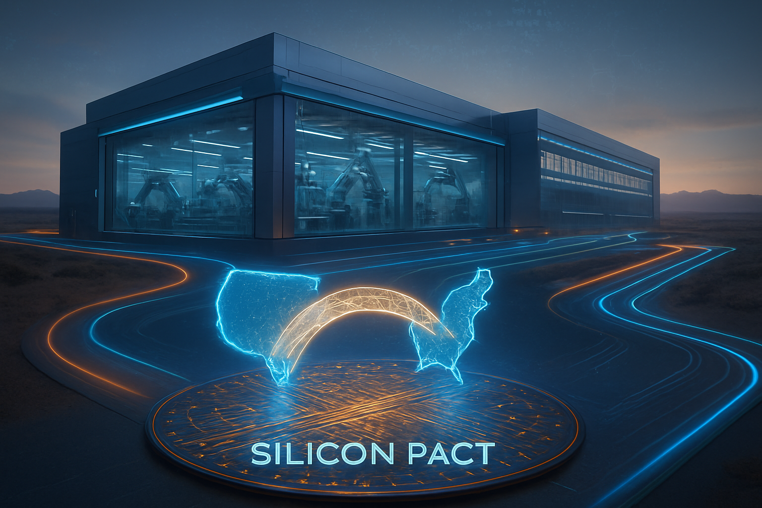
  • The Silicon Bridge: US and Taiwan Forge $500 Billion Pact to Secure the Global AI Supply Chain

    The Silicon Bridge: US and Taiwan Forge $500 Billion Pact to Secure the Global AI Supply Chain

    On January 13, 2026, the United States and Taiwan signed a monumental semiconductor trade and investment agreement that effectively rewrites the geography of the global artificial intelligence (AI) industry. This landmark "Silicon Pact," brokered by the U.S. Department of Commerce and the American Institute in Taiwan (AIT), establishes a $500 billion framework designed to reshore advanced chip manufacturing to American soil while reinforcing Taiwan's security through deep economic integration. At the heart of the deal is a staggering $250 billion credit guarantee provided by the Taiwanese government, specifically aimed at migrating the island’s vast ecosystem of small and medium-sized suppliers to new industrial clusters in the United States.

    The agreement marks a decisive shift from the "just-in-time" supply chain models of the previous decade to a "just-in-case" regionalized strategy. By incentivizing Taiwan Semiconductor Manufacturing Company (NYSE: TSM) to expand its Arizona footprint to as many as ten fabrication plants, the pact aims to produce 20% of the world's most advanced logic chips within U.S. borders by 2030. This development is not merely an industrial policy; it is a fundamental realignment of the "Silicon Shield," evolving it into a "Silicon Bridge" that binds the national security of the two nations through shared, high-tech infrastructure.

    The technical core of the agreement revolves around the massive $250 billion credit guarantee mechanism, a sophisticated public-private partnership managed by the Taiwanese National Development Fund (NDF) alongside major financial institutions like Cathay United Bank and Fubon Financial Holding Co. This fund is designed to solve the "clustering" problem: while giants like TSMC have the capital to expand globally, the thousands of specialized chemical, optics, and tool-making firms they rely on do not. The Taiwanese government will guarantee up to 60% of the loan value for these secondary suppliers, using a leverage multiple of 15x to 20x to ensure that the entire industrial ecosystem—not just the fabs—takes root in the U.S.

    In exchange for this massive capital injection, the U.S. has introduced the Tariff Offset Program (TOP). Under this program, reciprocal tariffs on Taiwanese goods have been reduced from 20% to 15%, placing Taiwan on the same trade tier as Japan and South Korea. Crucially, any chipmaker producing in the U.S. can now bypass the 25% global semiconductor surcharge, a penalty originally implemented to curb reliance on overseas manufacturing. To protect Taiwan’s domestic technological edge, the agreement formalizes the "N-2" principle: Taiwan commits to producing 2nm and 1.4nm chips in its Arizona facilities, provided that its domestic factories in Hsinchu and Kaohsiung remain at least two generations ahead in research and development.

    Initial reactions from the AI research community and industry experts have been overwhelmingly positive regarding the stability this brings to the "compute" layer of AI development. Dr. Arati Prabhakar, Director of the White House Office of Science and Technology Policy, noted that the pact "de-risks the most vulnerable point in the AI stack." However, some Taiwanese economists expressed concern that the migration of these suppliers could eventually lead to a "hollowing out" of the island’s domestic industry, a fear the Taiwanese government countered by emphasizing that the "Silicon Bridge" model makes Taiwan more indispensable to U.S. defense interests than ever before.

    The strategic implications for the world’s largest tech companies are profound. NVIDIA (NASDAQ: NVDA), the undisputed leader in AI hardware, stands as a primary beneficiary. By shifting its supply chain into the "safe harbor" of Arizona-based fabs, NVIDIA can maintain its industry-leading profit margins on H200 and Blackwell GPU clusters without the looming threat of sudden tariff hikes or regional instability. CEO Jensen Huang hailed the agreement as the "catalyst for the AI industrial revolution," noting that the deal provides the long-term policy certainty required for multi-billion dollar infrastructure bets.

    Apple (NASDAQ: AAPL) has also moved quickly to capitalize on the pact, reportedly securing over 50% of TSMC’s initial 2nm capacity in the United States. This ensures that future iterations of the iPhone and Mac—specifically the M6 and M7 series slated for 2027—will be powered by "Made in America" silicon. For Apple, this is a vital de-risking maneuver that satisfies both consumer demand for supply chain transparency and government pressure to reduce reliance on the Taiwan Strait. Similarly, AMD (NASDAQ: AMD) is restructuring its logistics to ensure its MI325X AI accelerators are produced within these new tariff-exempt zones, strengthening its competitive position against both NVIDIA and internal silicon efforts from cloud giants.

    Conversely, the deal places immense pressure on Intel (NASDAQ: INTC). Now led by CEO Lip-Bu Tan, Intel is being repositioned as a "national strategic asset" with the U.S. government maintaining a 10% stake in the company. While Intel must now compete directly with TSMC on U.S. soil for domestic talent and resources, the administration argues that this "domestic rivalry" will accelerate American engineering. The presence of a fully integrated Taiwanese ecosystem in the U.S. may actually benefit Intel by providing easier local access to the specialized materials and equipment that were previously only available in East Asia.

    Beyond the corporate balance sheets, this agreement represents a watershed moment in the broader AI landscape. We are witnessing the birth of "Sovereign AI Infrastructure," where national security and technological capability are inextricably linked. For decades, the "Silicon Shield" was a unilateral deterrent; it was the hope that the world’s need for Taiwanese chips would prevent a conflict. The transition to the "Silicon Bridge" suggests a more integrated, bilateral resilience model. By embedding Taiwan’s technological crown jewels within the American industrial base, the U.S. is signaling a permanent and material commitment to Taiwan’s security that goes beyond mere diplomatic rhetoric.

    The pact also addresses the growing concerns surrounding "AI Sovereignty." As AI models become the primary engines of economic growth, the physical locations where these models are trained and run—and where the chips that power them are made—have become matters of high statecraft. This deal effectively ensures that the Western AI ecosystem will have a stable, diversified source of high-end silicon regardless of geopolitical fluctuations in the Pacific. It mirrors previous historical milestones, such as the 1986 U.S.-Japan Semiconductor Agreement, but at a scale and speed that reflects the unprecedented urgency of the AI era.

    However, the "Silicon Bridge" is not without its critics. Human rights and labor advocates have raised concerns about the influx of thousands of Taiwanese workers into specialized "industrial parks" in Arizona and Texas, questioning whether U.S. labor laws and visa processes are prepared for such a massive, state-sponsored migration. Furthermore, some environmental groups have pointed to the extreme water and energy demands of the ten planned mega-fabs, urging the Department of Commerce to ensure that the $250 billion in credit guarantees includes strict sustainability mandates.

    Looking ahead, the next two to three years will be defined by the physical construction of this "bridge." We can expect to see a surge in specialized visa applications and the rapid development of "AI industrial zones" in the American Southwest. The near-term goal is to have the first 2nm production lines operational in Arizona by early 2027, followed closely by the migration of the secondary supply chain. This will likely trigger a secondary boom in American infrastructure, from specialized water treatment facilities to high-voltage power grids tailored for semiconductor manufacturing.

    Experts predict that if the "Silicon Bridge" model succeeds, it will serve as a blueprint for other strategic industries, such as high-capacity battery manufacturing and quantum computing. The challenge will be maintaining the "N-2" balance; if the technological gap between Taiwan and the U.S. closes too quickly, it could undermine the very security incentives that Taiwan is relying on. Conversely, if the U.S. facilities lag behind, the goal of supply chain resilience will remain unfulfilled. The Department of Commerce is expected to establish a permanent "Oversight Committee for Semiconductor Resilience" to monitor these technical benchmarks and manage the disbursement of the $250 billion in credit guarantees.

    The January 13 agreement is arguably the most significant piece of industrial policy in the 21st century. By combining $250 billion in direct corporate investment with a $250 billion state-backed credit guarantee, the U.S. and Taiwan have created a financial and geopolitical fortress around the AI supply chain. This pact does more than just build factories; it creates a deep, structural bond between two of the world's most critical technological hubs, ensuring that the silicon heart of the AI revolution remains protected and productive.

    The key takeaway is that the era of "stateless" technology is over. The "Silicon Bridge" signals a new age where the manufacturing of advanced AI chips is a matter of national survival, requiring unprecedented levels of international cooperation and financial intervention. In the coming months, the focus will shift from the high-level diplomatic signing to the "ground-breaking" phase—both literally and figuratively—as the first waves of Taiwanese suppliers begin their historic migration across the Pacific.


    This content is intended for informational purposes only and represents analysis of current AI developments.

    TokenRing AI delivers enterprise-grade solutions for multi-agent AI workflow orchestration, AI-powered development tools, and seamless remote collaboration platforms.
    For more information, visit https://www.tokenring.ai/.

  • The Glass Wall: Why Glass Substrates are the Newest Bottleneck in the AI Arms Race

    The Glass Wall: Why Glass Substrates are the Newest Bottleneck in the AI Arms Race

    As of January 20, 2026, the artificial intelligence industry has reached a pivotal juncture where software sophistication is once again being outpaced by the physical limitations of hardware. Following major announcements at CES 2026, it has become clear that the traditional organic substrates used to house the world’s most powerful chips have reached their breaking point. The industry is now racing toward a "Glass Age," as glass substrates emerge as the critical bottleneck determining which companies will dominate the next era of generative AI and sovereign supercomputing.

    The shift is not merely an incremental upgrade but a fundamental re-engineering of how chips are packaged. For decades, the industry relied on organic materials like Ajinomoto Build-up Film (ABF) to connect silicon to circuit boards. However, the massive thermal loads—often exceeding 1,000 watts—generated by modern AI accelerators have caused these organic materials to warp and fail. Glass, with its superior thermal stability and rigidity, has transitioned from a laboratory curiosity to the must-have architecture for the next generation of high-performance computing.

    The Technical Leap: Solving the Scaling Crisis

    The technical shift toward glass-core substrates is driven by three primary factors: thermal expansion, interconnect density, and structural integrity. Organic substrates possess a Coefficient of Thermal Expansion (CTE) that differs significantly from silicon, leading to mechanical stress and "warpage" as chips heat and cool. In contrast, glass can be engineered to match the CTE of silicon almost perfectly. This stability allows for the creation of massive, "reticle-busting" packages exceeding 100mm x 100mm, which are necessary to house the sprawling arrays of chiplets and HBM4 memory stacks that define 2026-era AI hardware.

    Furthermore, glass enables a 10x increase in through-glass via (TGV) density compared to the vias possible in organic layers. This allows for much finer routing—down to sub-2-micron line spacing—enabling faster data transfer between chiplets. Intel (NASDAQ: INTC) has taken an early lead in this space, announcing this month that its Xeon 6+ "Clearwater Forest" processor has officially entered High-Volume Manufacturing (HVM). This marks the first time a commercial CPU has utilized a glass-core substrate, proving that the technology is ready for the rigors of the modern data center.

    The reaction from the research community has been one of cautious optimism tempered by the reality of manufacturing yields. While glass offers unparalleled electrical performance and supports signaling speeds of up to 448 Gbps, its brittle nature makes it difficult to handle in the massive 600mm x 600mm panel formats used in modern factories. Initial yields are reported to be in the 75-85% range, significantly lower than the 95%+ yields common with organic substrates, creating an immediate supply-side bottleneck for the industry's largest players.

    Strategic Realignments: Winners and Losers

    The transition to glass is reshuffling the competitive hierarchy of the semiconductor world. Intel’s decade-long investment in glass research has granted it a significant first-mover advantage, potentially allowing it to regain market share in the high-end server market. Meanwhile, Samsung (KRX: 005930) has leveraged its expertise in display technology to form a "Triple Alliance" between its semiconductor, display, and electro-mechanics divisions. This vertical integration aims to provide a turnkey glass-substrate solution for custom AI ASICs by late 2026, positioning Samsung as a formidable rival to the traditional foundry models.

    TSMC (NYSE: TSM), the current king of AI chip manufacturing, finds itself in a more complex position. While it continues to dominate the market with its silicon-based CoWoS (Chip-on-Wafer-on-Substrate) technology for NVIDIA (NASDAQ: NVDA), TSMC's full-scale glass-based CoPoS (Chip-on-Panel-on-Substrate) platform is not expected to reach mass production until 2027 or 2028. This delay has created a strategic window for competitors and has forced companies like AMD (NASDAQ: AMD) to explore partnerships with SK Hynix (KRX: 000660) and its subsidiary, Absolics, which recently began shipping glass substrate samples from its new $600 million facility in Georgia.

    For AI startups and labs, this bottleneck means that the cost of compute is likely to remain high. As the industry moves away from commodity organic substrates toward specialized glass, the supply chain is tightening. The strategic advantage now lies with those who can secure guaranteed capacity from the few facilities capable of handling glass, such as those owned by Intel or the emerging SK Hynix-Absolics ecosystem. Companies that fail to pivot their chip architectures toward glass may find themselves literally unable to cool their next-generation designs.

    The Warpage Wall and Wider Significance

    The "Warpage Wall" is the hardware equivalent of the "Scaling Law" debate in AI software. Just as researchers question how much further LLMs can scale with existing data, hardware engineers have realized that AI performance cannot scale further with existing materials. The broader significance of glass substrates lies in their ability to act as a platform for Co-Packaged Optics (CPO). Because glass is transparent, it allows for the integration of optical interconnects directly into the chip package, replacing copper wires with light-speed data transmission—a necessity for the trillion-parameter models currently under development.

    However, this transition has exposed a dangerous single-source dependency in the global supply chain. The industry is currently reliant on a handful of specialized materials firms, most notably Nitto Boseki (TYO: 3110), which provides the high-end glass cloth required for these substrates. A projected 10-20% supply gap for high-grade glass materials in 2026 has sent shockwaves through the industry, drawing comparisons to the substrate shortages of 2021. This scarcity is turning glass from a technical choice into a geopolitical and economic lever.

    The move to glass also marks the final departure from the "Moore's Law" era of simple transistor scaling. We have entered the era of "System-on-Package," where the substrate is just as important as the silicon itself. Similar to the introduction of High Bandwidth Memory (HBM) or EUV lithography, the adoption of glass substrates represents a "no-turning-back" milestone. It is the foundation upon which the next decade of AI progress will be built, but it comes with the risk of further concentrating power in the hands of the few companies that can master its complex manufacturing.

    Future Horizons: Beyond the Pilot Phase

    Looking ahead, the next 24 months will be defined by the "yield race." While Intel is currently the only firm in high-volume manufacturing, Samsung and Absolics are expected to ramp up their production lines by the end of 2026. Experts predict that once yields stabilize above 90%, the industry will see a flood of new chip designs that take advantage of the 100mm+ package sizes glass allows. This will likely lead to a new class of "Super-GPUs" that combine dozens of chiplets into a single, massive compute unit.

    One of the most anticipated applications on the horizon is the integration of glass substrates into edge AI devices. While the current focus is on massive data center chips, the superior electrical properties of glass could eventually allow for thinner, more powerful AI-integrated laptops and smartphones. However, the immediate challenge remains the high cost of the specialized manufacturing equipment provided by firms like Applied Materials (NASDAQ: AMAT), which currently face a multi-year backlog for glass-processing tools.

    The Verdict on the Glass Transition

    The transition to glass substrates is more than a technical footnote; it is the physical manifestation of the AI industry's insatiable demand for power and speed. As organic materials fail under the heat of the AI revolution, glass provides the necessary structural and thermal foundation for the future. The current bottleneck is a symptom of a massive industrial pivot—one that favors first-movers like Intel and materials giants like Corning (NYSE: GLW) and Nitto Boseki.

    In summary, the next few months will be critical as more manufacturers transition from pilot samples to high-volume production. The industry must navigate a fragile supply chain and solve significant yield challenges to avoid a prolonged hardware shortage. For now, the "Glass Age" has officially begun, and it will be the defining factor in which AI architectures can survive the intense heat of the coming years. Keep a close eye on yield reports from the new Georgia and Arizona facilities; they will be the best indicators of whether the AI hardware train can keep its current momentum.


    This content is intended for informational purposes only and represents analysis of current AI developments.

    TokenRing AI delivers enterprise-grade solutions for multi-agent AI workflow orchestration, AI-powered development tools, and seamless remote collaboration platforms.
    For more information, visit https://www.tokenring.ai/.

  • OpenAI Signals End of the ‘Nvidia Tax’ with 2026 Launch of Custom ‘Titan’ Chip

    OpenAI Signals End of the ‘Nvidia Tax’ with 2026 Launch of Custom ‘Titan’ Chip

    In a decisive move toward vertical integration, OpenAI has officially unveiled the roadmap for its first custom-designed AI processor, codenamed "Titan." Developed in close collaboration with Broadcom (NASDAQ: AVGO) and slated for fabrication on Taiwan Semiconductor Manufacturing Company's (NYSE: TSM) cutting-edge N3 process, the chip represents a fundamental shift in OpenAI’s strategy. By moving from a software-centric model to a "fabless" semiconductor designer, the company aims to break its reliance on general-purpose hardware and gain direct control over the infrastructure powering its next generation of reasoning models.

    The announcement marks the formal pivot away from CEO Sam Altman's ambitious earlier discussions regarding a multi-trillion-dollar global foundry network. Instead, OpenAI is adopting what industry insiders call the "Apple Playbook," focusing on proprietary Application-Specific Integrated Circuit (ASIC) design to optimize performance-per-watt and, more critically, performance-per-dollar. With a target deployment date of December 2026, the Titan chip is engineered specifically to tackle the skyrocketing costs of inference—the phase where AI models generate responses—which have threatened to outpace the company’s revenue growth as models like the o1-series become more "thought-intensive."

    Technical Specifications: Optimizing for the Reasoning Era

    The Titan chip is not a general-purpose GPU meant to compete with Nvidia (NASDAQ: NVDA) across every possible workload; rather, it is a specialized ASIC fine-tuned for the unique architectural demands of Large Language Models (LLMs) and reasoning-heavy agents. Built on TSMC's 3-nanometer (N3) node, the Titan project leverages Broadcom's extensive library of intellectual property, including high-speed interconnects and sophisticated Ethernet switching. This collaboration is designed to create a "system-on-a-chip" environment that minimizes the latency between the processor and its high-bandwidth memory (HBM), a critical bottleneck in modern AI systems.

    Initial technical leaks suggest that Titan aims for a staggering 90% reduction in inference costs compared to existing general-purpose hardware. This is achieved by stripping away the legacy features required for graphics or scientific simulations—functions found in Nvidia’s Blackwell or Vera Rubin architectures—and focusing entirely on the "thinking cycles" required for autoregressive token generation. By optimizing the hardware specifically for OpenAI’s proprietary algorithms, Titan is expected to handle the "chain-of-thought" processing of future models with far greater energy efficiency than traditional GPUs.

    The AI research community has reacted with a mix of awe and skepticism. While many experts agree that custom silicon is the only way to scale inference to billions of users, others point out the risks of "architectural ossification." Because ASICs are hard-wired for specific tasks, a sudden shift in AI model architecture (such as a move away from Transformers) could render the Titan chip obsolete before it even reaches full scale. However, OpenAI’s decision to continue deploying Nvidia’s hardware alongside Titan suggests a "hybrid" strategy intended to mitigate this risk while lowering the baseline cost for their most stable workloads.

    Market Disruption: The Rise of the Hyperscaler Silicon

    The entry of OpenAI into the silicon market sends a clear message to the broader tech industry: the era of the "Nvidia tax" is nearing its end for the world’s largest AI labs. OpenAI joins an elite group of tech giants, including Google (NASDAQ: GOOGL) with its TPU v7 and Amazon (NASDAQ: AMZN) with its Trainium line, that are successfully decoupling their futures from third-party hardware vendors. This vertical integration allows these companies to capture the margins previously paid to semiconductor giants and gives them a strategic advantage in a market where compute capacity is the most valuable currency.

    For companies like Meta (NASDAQ: META), which is currently ramping up its own Meta Training and Inference Accelerator (MTIA), the Titan project serves as both a blueprint and a warning. The competitive landscape is shifting from "who has the best model" to "who can run the best model most cheaply." If OpenAI successfully hits its December 2026 deployment target, it could offer its API services at a price point that undercuts competitors who remain tethered to general-purpose GPUs. This puts immense pressure on mid-sized AI startups who lack the capital to design their own silicon, potentially widening the gap between the "compute-rich" and the "compute-poor."

    Broadcom stands as a major beneficiary of this shift. Despite a slight market correction in early 2026 due to lower initial margins on custom ASICs, the company has secured a massive $73 billion AI backlog. By positioning itself as the "architect for hire" for OpenAI and others, Broadcom has effectively cornered a new segment of the market: the custom AI silicon designer. Meanwhile, TSMC continues to act as the industry's ultimate gatekeeper, with its 3nm and 5nm nodes reportedly 100% booked through the end of 2026, forcing even the world’s most powerful companies to wait in line for manufacturing capacity.

    The Broader AI Landscape: From Foundries to Infrastructure

    The Titan project is the clearest indicator yet that the "trillions for foundries" narrative has evolved into a more pragmatic pursuit of "industrial infrastructure." Rather than trying to rebuild the global semiconductor supply chain from scratch, OpenAI is focusing its capital on what it calls the "Stargate" project—a $500 billion collaboration with Microsoft (NASDAQ: MSFT) and Oracle (NYSE: ORCL) to build massive data centers. Titan is the heart of this initiative, designed to fill these facilities with processors that are more efficient and less power-hungry than anything currently on the market.

    This development also highlights the escalating energy crisis within the AI sector. With OpenAI targeting a total compute commitment of 26 gigawatts, the efficiency of the Titan chip is not just a financial necessity but an environmental and logistical one. As power grids around the world struggle to keep up with the demands of AI, the ability to squeeze more "intelligence" out of every watt of electricity will become the primary metric of success. Comparisons are already being drawn to the early days of mobile computing, where proprietary silicon allowed companies like Apple to achieve battery life and performance levels that generic competitors could not match.

    However, the concentration of power remains a significant concern. By controlling the model, the software, and now the silicon, OpenAI is creating a closed ecosystem that could stifle open-source competition. If the most efficient way to run advanced AI is on proprietary hardware that is not for sale to the public, the "democratization of AI" may face its greatest challenge yet. The industry is watching closely to see if OpenAI will eventually license the Titan architecture or keep it strictly for internal use, further cementing its position as a sovereign entity in the tech world.

    Looking Ahead: The Roadmap to Titan 2 and Beyond

    The December 2026 launch of the first Titan chip is only the beginning. Sources indicate that OpenAI is already deep into the design phase for "Titan 2," which is expected to utilize TSMC’s A16 (1.6nm) process by 2027. This rapid iteration cycle suggests that OpenAI intends to match the pace of the semiconductor industry, releasing new hardware generations as frequently as it releases new model versions. Near-term, the focus will remain on stabilizing the N3 production yields and ensuring that the first racks of Titan servers are fully integrated into OpenAI’s existing data center clusters.

    In the long term, the success of Titan could pave the way for even more specialized hardware. We may see the emergence of "edge" versions of the Titan chip, designed to bring high-level reasoning capabilities to local devices without relying on the cloud. Challenges remain, particularly in the realm of global logistics and the ongoing geopolitical tensions surrounding semiconductor manufacturing in Taiwan. Any disruption to TSMC’s operations would be catastrophic for the Titan timeline, making supply chain resilience a top priority for Altman’s team as they move toward the late 2026 deadline.

    Experts predict that the next eighteen months will be a "hardware arms race" unlike anything seen since the early days of the PC. As OpenAI transitions from a software company to a hardware-integrated powerhouse, the boundary between "AI company" and "semiconductor company" will continue to blur. If Titan performs as promised, it will not only secure OpenAI’s financial future but also redefine the physical limits of what artificial intelligence can achieve.

    Conclusion: A New Chapter in AI History

    OpenAI's entry into the custom silicon market with the Titan chip marks a historic turning point. It is a calculated bet that the future of artificial intelligence belongs to those who own the entire stack, from the silicon atoms to the neural networks. By partnering with Broadcom and TSMC, OpenAI has bypassed the impossible task of building its own factories while still securing a customized hardware advantage that could last for years.

    The key takeaway for 2026 is that the AI industry has reached industrial maturity. No longer content with off-the-shelf solutions, the leaders of the field are now building the world they want to see, one transistor at a time. While the technical and geopolitical risks are substantial, the potential reward—a 90% reduction in the cost of intelligence—is too great to ignore. In the coming months, all eyes will be on TSMC’s fabrication schedules and the internal benchmarks of the first Titan prototypes, as the world waits to see if OpenAI can truly conquer the physical layer of the AI revolution.


    This content is intended for informational purposes only and represents analysis of current AI developments.

    TokenRing AI delivers enterprise-grade solutions for multi-agent AI workflow orchestration, AI-powered development tools, and seamless remote collaboration platforms.
    For more information, visit https://www.tokenring.ai/.

  • Silicon Dominance: TSMC Hits 2nm Mass Production Milestone as the Angstrom Era Arrives

    Silicon Dominance: TSMC Hits 2nm Mass Production Milestone as the Angstrom Era Arrives

    As of January 20, 2026, the global semiconductor landscape has officially entered a new epoch. Taiwan Semiconductor Manufacturing Company (NYSE: TSM) announced today that its 2-nanometer (N2) process technology has reached a critical mass production milestone, successfully ramping up high-volume manufacturing (HVM) at its lead facilities in Taiwan. This achievement marks the industry’s definitive transition into the "Angstrom Era," providing the essential hardware foundation for the next generation of generative AI models, autonomous systems, and ultra-efficient mobile computing.

    The milestone is characterized by "better than expected" yield rates and an aggressive expansion of capacity across TSMC’s manufacturing hubs. By hitting these targets in early 2026, TSMC has solidified its position as the primary foundry for the world’s most advanced silicon, effectively setting the pace for the entire technology sector. The move to 2nm is not merely a shrink in size but a fundamental shift in transistor architecture that promises to redefine the limits of power efficiency and computational density.

    The Nanosheet Revolution: Engineering the Future of Logic

    The 2nm node represents the most significant architectural departure for TSMC in over a decade: the transition from FinFET (Fin Field-Effect Transistor) to Nanosheet Gate-All-Around (GAAFET) transistors. In this new design, the gate surrounds the channel on all four sides, offering superior electrostatic control and virtually eliminating the electron leakage that had begun to plague FinFET designs at the 3nm barrier. Technical specifications released this month confirm that the N2 process delivers a 10–15% speed improvement at the same power level, or a staggering 25–30% power reduction at the same clock speed compared to the previous N3E node.

    A standout feature of this milestone is the introduction of NanoFlex™ technology. This innovation allows chip designers—including engineers at Apple (NASDAQ: AAPL) and NVIDIA (NASDAQ: NVDA)—to mix and match different nanosheet widths within a single chip design. This granular control allows specific sections of a processor to be optimized for extreme performance while others are tuned for power sipping, a capability that industry experts say is crucial for the high-intensity, fluctuating workloads of modern AI inference. Initial reports from the Hsinchu (Baoshan) "gigafab" and the Kaohsiung site indicate that yield rates for 2nm logic test chips have stabilized between 70% and 80%, a remarkably high figure for the early stages of such a complex architectural shift.

    Initial reactions from the semiconductor research community have been overwhelmingly positive. Dr. Aris Cheng, a senior analyst at the Global Semiconductor Alliance, noted, "TSMC's ability to maintain 70%+ yields while transitioning to GAAFET is a testament to their operational excellence. While competitors have struggled with the 'GAA learning curve,' TSMC appears to have bypassed the typical early-stage volatility." This reliability has allowed TSMC to secure massive volume commitments for 2026, ensuring that the next generation of flagship devices will be powered by 2nm silicon.

    The Competitive Gauntlet: TSMC, Intel, and Samsung

    The mass production milestone in January 2026 places TSMC in a fierce strategic position against its primary rivals. Intel (NASDAQ: INTC) has recently made waves with its 18A process, which technically beat TSMC to the market with backside power delivery—a feature Intel calls PowerVia. However, while Intel's Panther Lake chips have begun appearing in early 2026, analysts suggest that TSMC’s N2 node holds a significant lead in overall transistor density and manufacturing yield. TSMC is expected to introduce its own backside power delivery in the N2P node later this year, potentially neutralizing Intel's temporary advantage.

    Meanwhile, Samsung Electronics (KRX: 005930) continues to face challenges in its 2nm (SF2) ramp-up. Although Samsung was the first to adopt GAA technology at the 3nm stage, it has struggled to lure high-volume customers away from TSMC due to inconsistent yield rates and thermal management issues. As of early 2026, TSMC remains the "indispensable" foundry, with its 2nm capacity already reportedly overbooked by long-term partners like Advanced Micro Devices (NASDAQ: AMD) and MediaTek.

    For AI giants, this milestone is a sigh of relief. The massive demand for Blackwell-successor GPUs from NVIDIA and custom AI accelerators from hyperscalers like Alphabet Inc. (NASDAQ: GOOGL) and Microsoft (NASDAQ: MSFT) relies entirely on TSMC’s ability to scale. The strategic advantage of 2nm lies in its ability to pack more AI "neurons" into the same thermal envelope, a critical requirement for the massive data centers powering the 2026 era of LLMs.

    Global Footprints and the Arizona Timeline

    While the production heart of the 2nm era remains in Taiwan, TSMC has provided updated clarity on its international expansion, particularly in the United States. Following intense pressure from U.S. clients and the Department of Commerce, TSMC has accelerated its timeline for Fab 21 in Arizona. Phase 1 is already in high-volume production of 4nm chips, but Phase 2, which will focus on 3nm production, is now slated for mass production in the second half of 2027.

    More importantly, TSMC confirmed in January 2026 that Phase 3 of its Arizona site—the first U.S. facility planned for 2nm and the subsequent A16 (1.6nm) node—is on an "accelerated track." Groundbreaking occurred last year, and equipment installation is expected to begin in early 2027, with 2nm production on U.S. soil targeted for the 2028-2029 window. This geographic diversification is seen as a vital hedge against geopolitical instability in the Taiwan Strait, providing a "Silicon Shield" of sorts for the global AI economy.

    The wider significance of this milestone cannot be overstated. It marks a moment where the physical limits of materials science are being pushed to their absolute edge to sustain the momentum of the AI revolution. Comparisons are already being made to the 2011 transition to FinFET; just as that shift enabled the smartphone decade, the move to 2nm Nanosheets is expected to enable the decade of the "Ambient AI"—where high-performance intelligence is embedded in every device without the constraint of massive power cords.

    The Road to 14 Angstroms: What Lies Ahead

    Looking past the immediate success of the 2nm milestone, TSMC’s roadmap is already extending into the late 2020s. The company has teased the A14 (1.4nm) node, which is currently in the R&D phase at the Hsinchu research center. Near-term developments will include the "N2P" and "N2X" variants, which will integrate backside power delivery and enhanced voltage rails for the most demanding high-performance computing applications.

    However, challenges remain. The industry is reaching a point where traditional EUV (Extreme Ultraviolet) lithography may need to be augmented with High-NA (High Numerical Aperture) EUV machines—tools that cost upwards of $350 million each. TSMC has been cautious about adopting High-NA too early due to cost concerns, but the 2nm milestone suggests their current lithography strategy still has significant "runway." Experts predict that the next two years will be defined by a "density war," where the winner is decided not just by how small they can make a transistor, but by how many billions they can produce without defects.

    A New Benchmark for the Silicon Age

    The announcement of 2nm mass production in January 2026 is a watershed moment for the technology industry. It reaffirms TSMC’s role as the foundation of the modern digital world and provides the computational "fuel" needed for the next phase of artificial intelligence. By successfully navigating the transition to Nanosheet architecture and maintaining high yields in Hsinchu and Kaohsiung, TSMC has effectively set the technological standard for the next three to five years.

    In the coming months, the focus will shift from manufacturing milestones to product reveals. Consumers can expect the first 2nm-powered smartphones and laptops to be announced by late 2026, promising battery lives and processing speeds that were previously considered theoretical. For now, the "Angstrom Era" has arrived, and it is paved with Taiwanese silicon.


    This content is intended for informational purposes only and represents analysis of current AI developments.

    TokenRing AI delivers enterprise-grade solutions for multi-agent AI workflow orchestration, AI-powered development tools, and seamless remote collaboration platforms.
    For more information, visit https://www.tokenring.ai/.

  • The CoWoS Stranglehold: Why Advanced Packaging is the Kingmaker of the 2026 AI Economy

    The CoWoS Stranglehold: Why Advanced Packaging is the Kingmaker of the 2026 AI Economy

    As the AI revolution enters its most capital-intensive phase yet in early 2026, the industry’s greatest challenge is no longer just the design of smarter algorithms or the procurement of raw silicon. Instead, the global technology sector finds itself locked in a desperate scramble for "Advanced Packaging," specifically the Chip-on-Wafer-on-Substrate (CoWoS) technology pioneered by Taiwan Semiconductor Manufacturing Company (TSMC) (NYSE: TSM). While 2024 and 2025 were defined by the shortage of logic chips themselves, 2026 has seen the bottleneck shift entirely to the complex assembly process that binds massive compute dies to ultra-fast memory.

    This specialized manufacturing step is currently the primary throttle on global AI GPU supply, dictating the pace at which tech giants can build the next generation of "Super-Intelligence" clusters. With TSMC's CoWoS lines effectively sold out through the end of the year and premiums for "hot run" priority reaching record highs, the ability to secure packaging capacity has become the ultimate competitive advantage. For NVIDIA (NASDAQ: NVDA), Advanced Micro Devices (NASDAQ: AMD), and the hyperscalers developing their own custom silicon, the battle for 2026 isn't being fought in the design lab, but on the factory floors of automated backend facilities in Taiwan.

    The Technical Crucible: CoWoS-L and the HBM4 Integration Challenge

    At the heart of this manufacturing crisis is the sheer physical complexity of modern AI hardware. As of January 2026, NVIDIA’s newly unveiled Rubin R100 GPUs and its predecessor, the Blackwell B200, have pushed silicon manufacturing to its theoretical limits. Because these chips are now larger than a single "reticle" (the maximum size a lithography machine can print in one pass), TSMC must use CoWoS-L technology to stitch together multiple chiplets using silicon bridges. This process allows for a massive "Super-Chip" architecture that behaves as a single unit but requires microscopic precision to assemble, leading to lower yields and longer production cycles than traditional monolithic chips.

    The integration of sixth-generation High Bandwidth Memory (HBM4) has further complicated the technical landscape. Rubin chips require the integration of up to 12 stacks of HBM4, which utilize a 2048-bit interface—double the width of previous generations. This requires a staggering density of vertical and horizontal interconnects that are highly sensitive to thermal warpage during the bonding process. To combat this, TSMC has transitioned to "Hybrid Bonding" techniques, which eliminate traditional solder bumps in favor of direct copper-to-copper connections. While this increases performance and reduces heat, it demands a "clean room" environment that rivals the purity of front-end wafer fabrication, essentially turning "packaging"—historically a low-tech backend process—into a high-stakes extension of the foundry itself.

    Industry experts and researchers at the International Solid-State Circuits Conference (ISSCC) have noted that this shift represents the most significant change in semiconductor manufacturing in two decades. Previously, the industry relied on "Moore's Law" through transistor scaling; today, we have entered the era of "System-on-Integrated-Chips" (SoIC). The consensus among the research community is that the packaging is no longer just a protective shell but an integral part of the compute engine. If the interposer or the bridge fails, the entire $40,000 GPU becomes a multi-thousand-dollar paperweight, making yield management the most guarded secret in the industry.

    The Corporate Arms Race: Anchor Tenants and Emerging Rivals

    The strategic implications of this capacity shortage are reshaping the hierarchy of Big Tech. NVIDIA remains the "anchor tenant" of TSMC’s advanced packaging ecosystem, reportedly securing nearly 60% of total CoWoS output for 2026 to support its shift to a relentless 12-month release cycle. This dominant position has forced competitors like AMD and Broadcom (NASDAQ: AVGO)—which produces custom AI TPUs for Google and Meta—to fight over the remaining 40%. The result is a tiered market where the largest players can maintain a predictable roadmap, while smaller AI startups and "Sovereign AI" initiatives by national governments face lead times exceeding nine months for high-end hardware.

    In response to the TSMC bottleneck, a secondary market for advanced packaging is rapidly maturing. Intel Corporation (NASDAQ: INTC) has successfully positioned its "Foveros" and EMIB packaging technologies as a viable alternative for companies looking to de-risk their supply chains. In early 2026, Microsoft and Amazon have reportedly diverted some of their custom silicon orders to Intel's US-based packaging facilities in New Mexico and Arizona, drawn by the promise of "Sovereign AI" manufacturing. Meanwhile, Samsung Electronics (KRX: 005930) is aggressively marketing its "turnkey" solution, offering to provide both the HBM4 memory and the I-Cube packaging in a single contract—a move designed to undercut TSMC’s fragmented supply chain where memory and packaging are often handled by different entities.

    The strategic advantage for 2026 belongs to those who have vertically integrated or secured long-term capacity agreements. Companies like Amkor Technology (NASDAQ: AMKR) have seen their stock soar as they take on "overflow" 2.5D packaging tasks that TSMC no longer has the bandwidth to handle. However, the reliance on Taiwan remains the industry's greatest vulnerability. While TSMC is expanding into Arizona and Japan, those facilities are still primarily focused on wafer fabrication; the most advanced CoWoS-L and SoIC assembly remains concentrated in Taiwan's AP6 and AP7 fabs, leaving the global AI economy tethered to the geopolitical stability of the Taiwan Strait.

    A Choke Point Within a Choke Point: The Broader AI Landscape

    The 2026 CoWoS crisis is a symptom of a broader trend: the "physicalization" of the AI boom. For years, the narrative around AI focused on software, neural network architectures, and data. Today, the limiting factor is the physical reality of atoms, heat, and microscopic wires. This packaging bottleneck has effectively created a "hard ceiling" on the growth of the global AI compute capacity. Even if the world could build a dozen more "Giga-fabs" to print silicon wafers, they would still sit idle without the specialized "pick-and-place" and bonding equipment required to finish the chips.

    This development has profound impacts on the AI landscape, particularly regarding the cost of entry. The capital expenditure required to secure a spot in the CoWoS queue is so high that it is accelerating the consolidation of AI power into the hands of a few trillion-dollar entities. This "packaging tax" is being passed down to consumers and enterprise clients, keeping the cost of training Large Language Models (LLMs) high and potentially slowing the democratization of AI. Furthermore, it has spurred a new wave of innovation in "packaging-efficient" AI, where researchers are looking for ways to achieve high performance using smaller, more easily packaged chips rather than the massive "Super-Chips" that currently dominate the market.

    Comparatively, the 2026 packaging crisis mirrors the oil shocks of the 1970s—a realization that a vital global resource is controlled by a tiny number of suppliers and subject to extreme physical constraints. This has led to a surge in government subsidies for "Backend" manufacturing, with the US CHIPS Act and similar European initiatives finally prioritizing packaging plants as much as wafer fabs. The realization has set in: a chip is not a chip until it is packaged, and without that final step, the "Silicon Intelligence" remains trapped in the wafer.

    Looking Ahead: Panel-Level Packaging and the 2027 Roadmap

    The near-term solution to the 2026 bottleneck involves the massive expansion of TSMC’s Advanced Backend Fab 7 (AP7) in Chiayi and the repurposing of former display panel plants for "AP8." However, the long-term future of the industry lies in a transition from Wafer-Level Packaging to Fan-Out Panel-Level Packaging (FOPLP). By using large rectangular panels instead of circular 300mm wafers, manufacturers can increase the number of chips processed in a single batch by up to 300%. TSMC and its partners are already conducting pilot runs for FOPLP, with expectations that it will become the high-volume standard by late 2027 or 2028.

    Another major hurdle on the horizon is the transition to "Glass Substrates." As the number of chiplets on a single package increases, the organic substrates currently in use are reaching their limits of structural integrity and electrical performance. Intel has taken an early lead in glass substrate research, which could allow for even denser interconnects and better thermal management. If successful, this could be the catalyst that allows Intel to break TSMC's packaging monopoly in the latter half of the decade. Experts predict that the winner of the "Glass Race" will likely dominate the 2028-2030 AI hardware cycle.

    Conclusion: The Final Frontier of Moore's Law

    The current state of advanced packaging represents a fundamental shift in the history of computing. As of January 2026, the industry has accepted that the future of AI does not live on a single piece of silicon, but in the sophisticated "cities" of chiplets built through CoWoS and its successors. TSMC’s ability to scale this technology has made it the most indispensable company in the world, yet the extreme concentration of this capability has created a fragile equilibrium for the global economy.

    For the coming months, the industry will be watching two key indicators: the yield rates of HBM4 integration and the speed at which TSMC can bring its AP7 Phase 2 capacity online. Any delay in these areas will have a cascading effect, delaying the release of next-generation AI models and cooling the current investment cycle. In the 2020s, we learned that data is the new oil; in 2026, we are learning that advanced packaging is the refinery. Without it, the "crude" silicon of the AI revolution remains useless.


    This content is intended for informational purposes only and represents analysis of current AI developments.

    TokenRing AI delivers enterprise-grade solutions for multi-agent AI workflow orchestration, AI-powered development tools, and seamless remote collaboration platforms.
    For more information, visit https://www.tokenring.ai/.
  • The Silicon Glue: 2026 HBM4 Sampling and the Global Alliance Ending the AI Memory Bottleneck

    The Silicon Glue: 2026 HBM4 Sampling and the Global Alliance Ending the AI Memory Bottleneck

    As of January 19, 2026, the artificial intelligence industry is witnessing an unprecedented capital expenditure surge centered on a single, critical component: High-Bandwidth Memory (HBM). With the transition from HBM3e to the revolutionary HBM4 standard reaching a fever pitch, the "memory wall"—the performance gap between ultra-fast logic processors and slower data storage—is finally being dismantled. This shift is not merely an incremental upgrade but a structural realignment of the semiconductor supply chain, led by a powerhouse alliance between SK Hynix (KRX: 000660), TSMC (NYSE: TSM), and NVIDIA (NASDAQ: NVDA).

    The immediate significance of this development cannot be overstated. As large-scale AI models move toward the 100-trillion parameter threshold, the ability to feed data to GPUs has become the primary constraint on performance. The massive investments announced this month by the world’s leading memory makers indicate that the industry has entered a "supercycle" phase, where HBM is no longer treated as a commodity but as a customized, high-value logic component essential for the survival of the AI era.

    The HBM4 Revolution: 2048-bit Interfaces and Active Memory

    The HBM4 transition, currently entering its critical sampling phase in early 2026, represents the most significant architectural change in memory technology in over a decade. Unlike HBM3e, which utilized a 1024-bit interface, HBM4 doubles the bus width to a staggering 2048-bit interface. This "wider pipe" allows for massive data throughput—targeted at up to 3.25 TB/s per stack—without requiring the extreme clock speeds that have plagued previous generations with thermal and power efficiency issues. By doubling the interface width, manufacturers can achieve higher performance at lower power consumption, a critical factor for the massive AI "factories" being built by hyperscalers.

    Furthermore, the introduction of "active" memory marks a radical departure from traditional DRAM manufacturing. For the first time, the base die (or logic die) at the bottom of the HBM stack is being manufactured using advanced logic nodes rather than standard memory processes. SK Hynix has formally partnered with TSMC to produce these base dies on 5nm and 12nm processes. This allows the memory stack to gain "active" processing capabilities, effectively embedding basic logic functions directly into the memory. This "processing-near-memory" approach enables the HBM stack to handle data manipulation and sorting before it even reaches the GPU, significantly reducing latency.

    Initial reactions from the AI research community have been overwhelmingly positive. Experts suggest that the move to a 2048-bit interface and TSMC-manufactured logic dies will provide the 3x to 5x performance leap required for the next generation of multimodal AI agents. By integrating the memory and logic more closely through hybrid bonding techniques, the industry is effectively moving toward "3D Integrated Circuits," where the distinction between where data is stored and where it is processed begins to blur.

    A Three-Way Race: Market Share and Strategic Alliances

    The strategic landscape of 2026 is defined by a fierce three-way race for HBM dominance among SK Hynix, Samsung (KRX: 005930), and Micron (NASDAQ: MU). SK Hynix currently leads the market with a dominant share estimated between 53% and 62%. The company recently announced that its entire 2026 HBM capacity is already fully booked, primarily by NVIDIA for its upcoming Rubin architecture and Blackwell Ultra series. SK Hynix’s "One Team" alliance with TSMC has given it a first-mover advantage in the HBM4 generation, allowing it to provide a highly optimized "active" memory solution that competitors are now scrambling to match.

    However, Samsung is mounting a massive recovery effort. After a delayed start in the HBM3e cycle, Samsung successfully qualified its 12-layer HBM3e for NVIDIA in late 2025 and is now targeting a February 2026 mass production start for its own HBM4 stacks. Samsung’s primary strategic advantage is its "turnkey" capability; as the only company that owns both world-class DRAM production and an advanced semiconductor foundry, Samsung can produce the HBM stacks and the logic dies entirely in-house. This vertical integration could theoretically offer lower costs and tighter design cycles once their 4nm logic die yields stabilize.

    Meanwhile, Micron has solidified its position as a critical third pillar in the supply chain, controlling approximately 15% to 21% of the market. Micron’s aggressive move to establish a "Megafab" in New York and its early qualification of 12-layer HBM3e have made it a preferred partner for companies seeking to diversify their supply away from the SK Hynix/TSMC duopoly. For NVIDIA and AMD (NASDAQ: AMD), this fierce competition is a massive benefit, ensuring a steady supply of high-performance silicon even as demand continues to outstrip supply. However, smaller AI startups may face a "memory drought," as the "Big Three" have largely prioritized long-term contracts with trillion-dollar tech giants.

    Beyond the Memory Wall: Economic and Geopolitical Shifts

    The massive investment in HBM fits into a broader trend of "hardware-software co-design" that is reshaping the global tech landscape. As AI models transition from static LLMs into proactive agents capable of real-world reasoning, the "Memory Wall" has replaced raw compute power as the most significant hurdle for AI scaling. The 2026 HBM surge reflects a realization across the industry that the bottleneck for artificial intelligence is no longer just FLOPS (floating-point operations per second), but the "communication cost" of moving data between memory and logic.

    The economic implications are profound, with the total HBM market revenue projected to reach nearly $60 billion in 2026. This is driving a significant relocation of the semiconductor supply chain. SK Hynix’s $4 billion investment in an advanced packaging plant in Indiana, USA, and Micron’s domestic expansion represent a strategic shift toward "onshoring" critical AI components. This move is partly driven by the need to be closer to US-based design houses like NVIDIA and partly by geopolitical pressures to secure the AI supply chain against regional instabilities.

    However, the concentration of this technology in the hands of just three memory makers and one leading foundry (TSMC) raises concerns about market fragility. The high cost of entry—requiring billions in specialized "Advanced Packaging" equipment and cleanrooms—means that the barrier to entry for new competitors is nearly insurmountable. This reinforces a global "AI arms race" where nations and companies without direct access to the HBM4 supply chain may find themselves technologically sidelined as the gap between state-of-the-art AI and "commodity" AI continues to widen.

    The Road to Half-Terabyte GPUs and HBM5

    Looking ahead through the remainder of 2026 and into 2027, the industry expects the first volume shipments of 16-layer (16-Hi) HBM4 stacks. These stacks are expected to provide up to 64GB of memory per "cube." In an 8-stack configuration—which is rumored for NVIDIA’s upcoming Rubin platform—a single GPU could house a staggering 512GB of high-speed memory. This would allow researchers to train and run massive models on significantly smaller hardware footprints, potentially enabling "Sovereign AI" clusters that occupy a fraction of the space of today's data centers.

    The primary technical challenge remaining is heat dissipation. As memory stacks grow taller and logic dies become more powerful, managing the thermal profile of a 16-layer stack will require breakthroughs in liquid-to-chip cooling and hybrid bonding techniques that eliminate the need for traditional "bumps" between layers. Experts predict that if these thermal hurdles are cleared, the industry will begin looking toward HBM4E (Extended) by late 2027, which will likely integrate even more complex AI accelerators directly into the memory base.

    Beyond 2027, the roadmap for HBM5 is already being discussed in research circles. Early predictions suggest HBM5 may transition from electrical interconnects to optical interconnects, using light to move data between the memory and the processor. This would essentially eliminate the bandwidth bottleneck forever, but it requires a fundamental rethink of how silicon chips are designed and manufactured.

    A Landmark Shift in Semiconductor History

    The HBM explosion of 2026 is a watershed moment for the semiconductor industry. By breaking the memory wall, the triad of SK Hynix, TSMC, and NVIDIA has paved the way for a new era of AI capability. The transition to HBM4 marks the point where memory stopped being a passive storage bin and became an active participant in computation. The shift from commodity DRAM to customized, logic-integrated HBM is the most significant change in memory architecture since the invention of the integrated circuit.

    In the coming weeks and months, the industry will be watching Samsung’s production yields at its Pyeongtaek campus and the initial performance benchmarks of the first HBM4 engineering samples. As 2026 progresses, the success of these HBM4 rollouts will determine which tech giants lead the next decade of AI innovation. The memory bottleneck is finally yielding, and with it, the limits of what artificial intelligence can achieve are being redefined.


    This content is intended for informational purposes only and represents analysis of current AI developments.

    TokenRing AI delivers enterprise-grade solutions for multi-agent AI workflow orchestration, AI-powered development tools, and seamless remote collaboration platforms.
    For more information, visit https://www.tokenring.ai/.