As the global technology industry crosses into 2026, ASML (NASDAQ:ASML) has officially cemented its role as the ultimate gatekeeper of the artificial intelligence revolution. Following a fiscal 2025 that saw unprecedented demand for AI-specific silicon, ASML’s 2026 outlook points to a historic revenue target of €36.5 billion. This growth is being propelled by a massive capital expenditure surge from industry titans Intel (NASDAQ:INTC) and TSMC (NYSE:TSM), who are locked in a high-stakes "Race to 2nm" and beyond. The centerpiece of this transformation is the transition of High-NA (Numerical Aperture) Extreme Ultraviolet (EUV) lithography from experimental pilot lines into high-volume manufacturing (HVM).
The immediate significance of this development cannot be overstated. With Big Tech projected to invest over $400 billion in AI infrastructure in 2026 alone, the bottleneck has shifted from software algorithms to the physical limits of silicon. ASML’s delivery of the Twinscan EXE:5200 systems represents the first time the semiconductor industry can reliably print features at the angstrom scale in a commercial environment. This technological leap is the primary engine allowing chipmakers to keep pace with the exponential compute requirements of next-generation Large Language Models (LLMs) and autonomous AI agents.
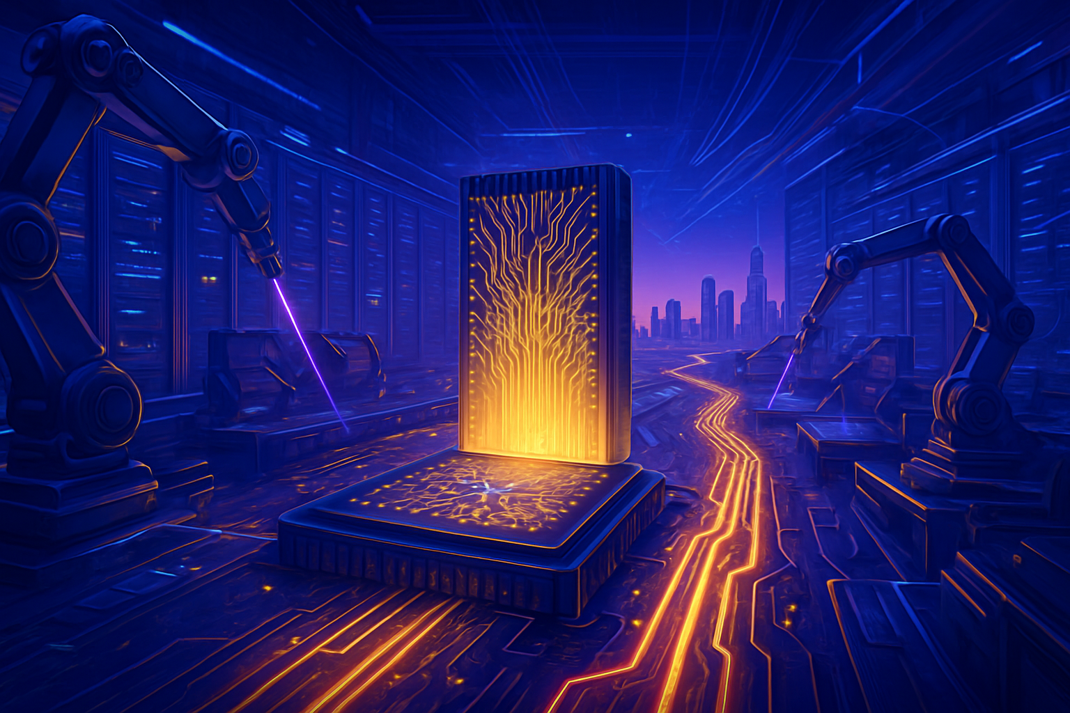
The Technical Edge: Twinscan EXE:5200 and the 8nm Resolution Frontier
At the heart of the 2026 roadmap is the Twinscan EXE:5200, ASML’s flagship High-NA EUV system. Unlike the previous generation of standard (Low-NA) EUV tools that utilized a 0.33 numerical aperture, the High-NA systems utilize a 0.55 NA lens system. This allows for a resolution of 8nm, enabling the printing of features that are 1.7 times smaller than what was previously possible. For engineers, this means the ability to achieve a 2.9x increase in transistor density without the need for complex, yield-killing multi-patterning techniques.
The EXE:5200 is a significant upgrade over the R&D-focused EXE:5000 models delivered in 2024 and 2025. It boasts a productivity throughput of over 200 wafers per hour (WPH), matching the efficiency of standard EUV tools while operating at a far tighter resolution. This throughput is critical for the commercial viability of 2nm and 1.4nm (14A) nodes. By moving to a single-exposure process for the most critical metal layers of a chip, manufacturers can reduce cycle times and minimize the cumulative defects that occur when a single layer must be passed through a scanner multiple times.
Initial reactions from the industry have been polarized along strategic lines. Intel, which received the world’s first commercial-grade EXE:5200B in late 2025, has championed the tool as the "holy grail" of process leadership. Conversely, experts at TSMC initially expressed caution regarding the system's $400 million price tag, preferring to push standard EUV to its absolute limits. However, as of early 2026, the sheer complexity of 1.6nm (A16) and 1.4nm designs has forced a universal consensus: High-NA is no longer an optional luxury but a fundamental requirement for the "Angstrom Era."
Strategic Warfare: Intel’s First-Mover Gamble vs. TSMC’s Efficiency Engine
The competitive landscape of 2026 is defined by a sharp divergence in how the world’s two largest foundries are deploying ASML’s technology. Intel has adopted an aggressive "first-mover" strategy, utilizing High-NA EUV to accelerate its 14A (1.4nm) node. By integrating these tools earlier than its rivals, Intel aims to reclaim the process leadership it lost a decade ago. For Intel, 2026 is the "prove-it" year; if the EXE:5200 can deliver superior yields for its Panther Lake and Clearwater Forest processors, the company will have a strategic advantage in attracting external foundry customers like Microsoft (NASDAQ:MSFT) and Nvidia (NASDAQ:NVDA).
TSMC, meanwhile, is operating with a massive 2026 capex budget of $52 billion to $56 billion, much of which is dedicated to the high-volume ramp of its N2 (2nm) and N2P nodes. While TSMC has been more conservative with High-NA adoption—relying on standard EUV with advanced multi-patterning for its A16 (1.6nm) process—the company has begun installing High-NA evaluation tools in early 2026 to de-risk its future A10 node. TSMC’s strategy focuses on maximizing the ROI of its existing EUV fleet while maintaining its dominant 90% market share in high-end AI accelerators.
This shift has profound implications for chip designers. Nvidia’s "Rubin" R100 architecture and AMD’s (NASDAQ:AMD) MI400 series, both expected to dominate 2026 data center sales, are being optimized for these new nodes. While Nvidia is currently leveraging TSMC’s 3nm N3P process, rumors suggest a split-foundry strategy may emerge by the end of 2026, with some high-performance components being shifted to Intel’s 18A or 14A lines to ensure supply chain resiliency.
The Triple Threat: 2nm, Advanced Packaging, and the Memory Supercycle
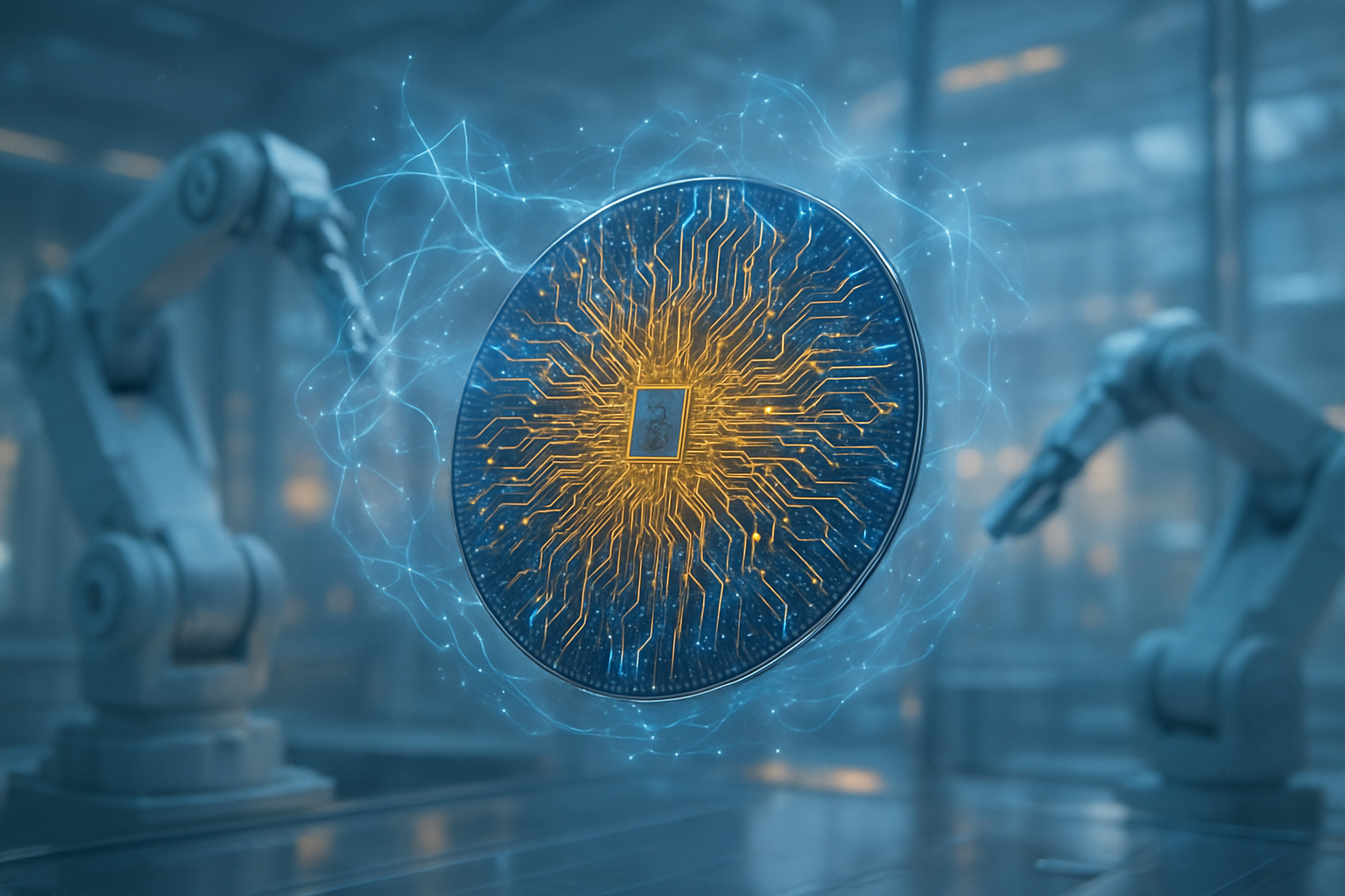
The 2026 outlook is not merely about smaller transistors; it is about "System-on-Package" (SoP) innovation. Advanced packaging has become a third growth lever for ASML. Techniques like TSMC’s CoWoS-L (Chip-on-Wafer-on-Substrate with Local Silicon Interconnect) are now scaling to 5.5x the reticle limit, allowing for massive AI "Super-Chips" that combine logic, cache, and HBM4 (High Bandwidth Memory) in a single massive footprint. ASML has responded by launching specialized scanners like the Twinscan XT:260, designed specifically for the high-precision alignment required in 3D stacking and hybrid bonding.
The memory sector is also becoming an "EUV-intensive" business. SK Hynix (KRX:000660) and Samsung (KRX:005930) are in the midst of an HBM-led supercycle, where the logic base dies for HBM4 are being manufactured on advanced logic nodes (5nm and 12nm). This has created a secondary surge in orders for ASML’s standard EUV systems. For the first time in history, the demand for lithography tools is being driven equally by memory density and logic performance, creating a diversified revenue stream that insulates ASML from downturns in the consumer smartphone or PC markets.
However, this transition is not without concerns. The extreme cost of High-NA systems and the energy required to run them are putting pressure on the margins of smaller players. Industry analysts worry that the "Angstrom Era" may lead to further consolidation, as only a handful of companies can afford the $20+ billion price tag of a modern "Mega-Fab." Geopolitical tensions also remain a factor, as ASML continues to navigate strict export controls that have drastically reduced its revenue from China, forcing the company to rely even more heavily on the U.S., Taiwan, and South Korea.
Future Horizons: The Path to 1nm and the Glass Substrate Pivot
Looking beyond 2026, the trajectory for lithography points toward the sub-1nm frontier. ASML is already in the early R&D phases for "Hyper-NA" systems, which would push the numerical aperture to 0.75. Near-term, we expect to see the full stabilization of High-NA yields by the third quarter of 2026, followed by the first 1.4nm (14A) risk production runs. These developments will be essential for the next generation of AI hardware capable of on-device "reasoning" and real-time multimodal processing.
Another development to watch is the shift toward glass substrates. Led by Intel, the industry is beginning to replace organic packaging materials with glass to provide the structural integrity needed for the increasingly heavy and hot AI chip stacks. ASML’s packaging-specific lithography tools will play a vital role here, ensuring that the interconnects on these glass substrates can meet the nanometer-perfect alignment required for copper-to-copper hybrid bonding. Experts predict that by 2028, the distinction between "front-end" wafer fabrication and "back-end" packaging will have blurred entirely into a single, continuous manufacturing flow.
Conclusion: ASML’s Indispensable Decade
As we move through 2026, ASML stands at the center of the most aggressive capital expansion in industrial history. The transition to High-NA EUV with the Twinscan EXE:5200 is more than just a technical milestone; it is the physical foundation upon which the next decade of artificial intelligence will be built. With a €33 billion order backlog and a dominant position in both logic and memory lithography, ASML is uniquely positioned to benefit from the "AI Infrastructure Supercycle."
The key takeaway for 2026 is that the industry has successfully navigated the "air pocket" of the early 2020s and is now entering a period of normalized, high-volume growth. While the "Race to 2nm" will produce clear winners and losers among foundries, the collective surge in capex ensures that the compute bottleneck will continue to widen, making way for AI models of unprecedented scale. In the coming months, the industry will be watching Intel’s 18A yield reports and TSMC’s A16 progress as the definitive indicators of who will lead the angstrom-scale future.
This content is intended for informational purposes only and represents analysis of current AI developments.
TokenRing AI delivers enterprise-grade solutions for multi-agent AI workflow orchestration, AI-powered development tools, and seamless remote collaboration platforms.
For more information, visit https://www.tokenring.ai/.