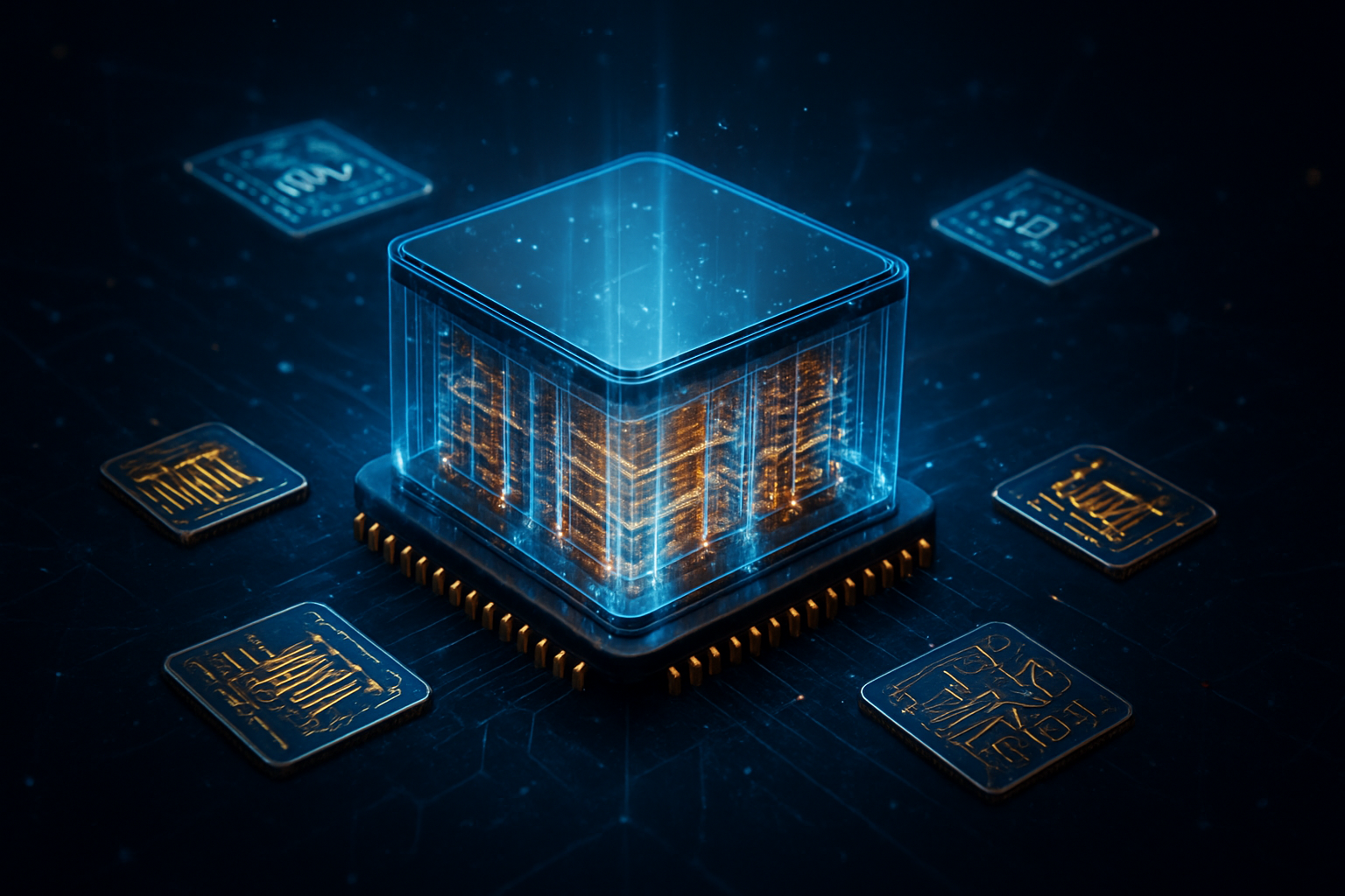
The semiconductor industry is undergoing its most significant architectural transformation since the invention of the integrated circuit. As of February 2026, the era of massive, monolithic processors—where every component of a chip is etched onto a single, giant piece of silicon—is rapidly giving way to a modular "Silicon Lego" approach. At the heart of this revolution is the Universal Chiplet Interconnect Express (UCIe) standard, an open industry specification that allows different silicon "chiplets" to be mixed, matched, and stacked within a single package with the same ease as plugging a USB drive into a laptop.
This shift is not merely a technical curiosity; it is a fundamental survival strategy for the AI era. With the physical limits of traditional manufacturing (the so-called "reticle limit") making it impossible to build larger chips, and the costs of 2nm and 1.4nm nodes skyrocketing, modularity has become the only viable path to power the next generation of trillion-parameter AI models. By standardizing how these tiny pieces of silicon communicate, the UCIe Consortium is enabling a new world of heterogeneous integration, where specialized AI accelerators from one vendor can sit directly alongside high-performance CPUs and memory from others.
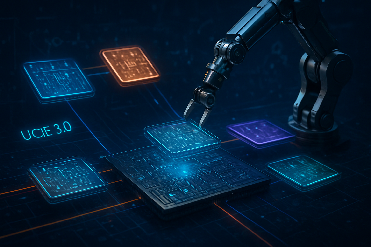
The Dawn of "Silicon Lego": UCIe 3.0 and the Modular Mandate
The current state of the art, defined by the UCIe 3.0 specification released in late 2025, has effectively doubled the performance ceiling of its predecessors. Operating at data rates of up to 64 GT/s per lane, UCIe 3.0 provides a massive shoreline bandwidth of over 2,600 GB/s per millimeter. This performance level is critical for AI workloads, where the movement of data between compute cores and memory is often the primary bottleneck. Unlike previous proprietary interconnects, UCIe is designed for ultra-low latency, comparable to the internal wiring of a monolithic chip, while achieving power efficiency as low as 0.01 pJ/bit in advanced 3D packaging configurations.
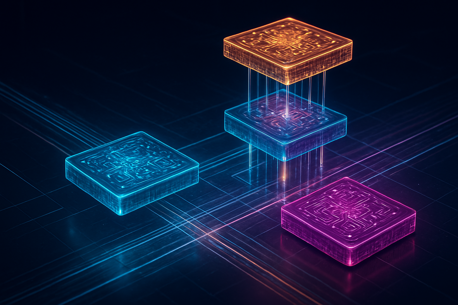
This technical leap differs from previous approaches by decoupling the manufacturing process for different parts of a chip. In a modern AI superchip, a company can now use the most expensive, cutting-edge 1.8nm process from Intel (NASDAQ: INTC) or TSMC (NYSE: TSM) for the critical compute logic, while keeping the I/O and analog components on more mature, cost-effective 5nm or 7nm nodes. This "mix and match" capability has been met with overwhelming support from the AI research community, as it allows for the creation of domain-specific accelerators (DSAs) that can be swapped into a standard package without redesigning the entire system.
Navigating the Competitive Tides: Strategic Shifts for Tech Giants
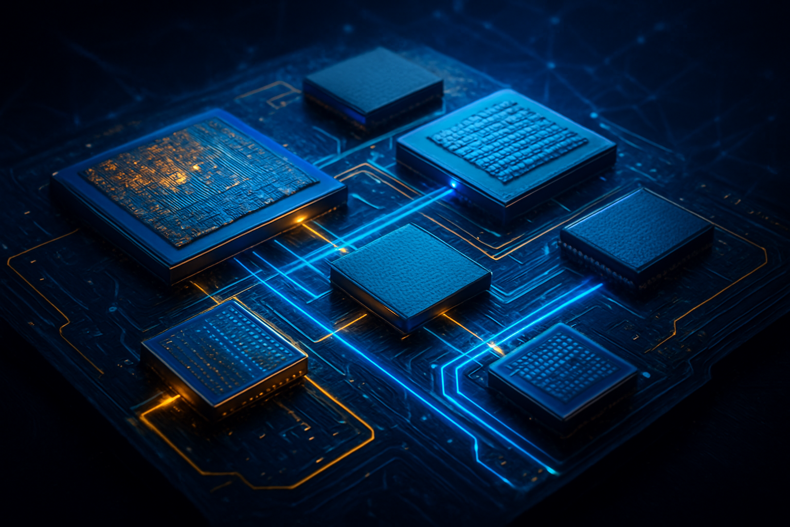
The rise of UCIe has created a complex new competitive landscape. Intel has been a primary driver of the standard, using it to underpin its "System Foundry" model. By opening its world-class packaging facilities to third-party chiplets, Intel aims to become the universal hub for the entire industry. Meanwhile, AMD (NASDAQ: AMD), a pioneer in chiplet design, has integrated UCIe to broaden its ecosystem while maintaining its proprietary Infinity Fabric for internal low-latency links. Even NVIDIA (NASDAQ: NVDA), which traditionally maintained a "walled garden" with its NVLink technology, has begun integrating UCIe IP to allow its partners to plug custom ASICs and optical interconnects directly into the NVIDIA ecosystem.
This modularity is particularly disruptive for hyperscalers like Alphabet Inc. (NASDAQ: GOOGL), Meta Platforms, Inc. (NASDAQ: META), and Microsoft Corporation (NASDAQ: MSFT). These companies are now increasingly designing their own specialized AI chiplets—custom NPUs optimized for their specific software stacks—and "snapping" them into packages produced by established foundries. This reduces their reliance on off-the-shelf silicon and cuts development costs by an estimated 40%, potentially shifting the balance of power from traditional chip designers to the cloud giants who consume the most silicon.
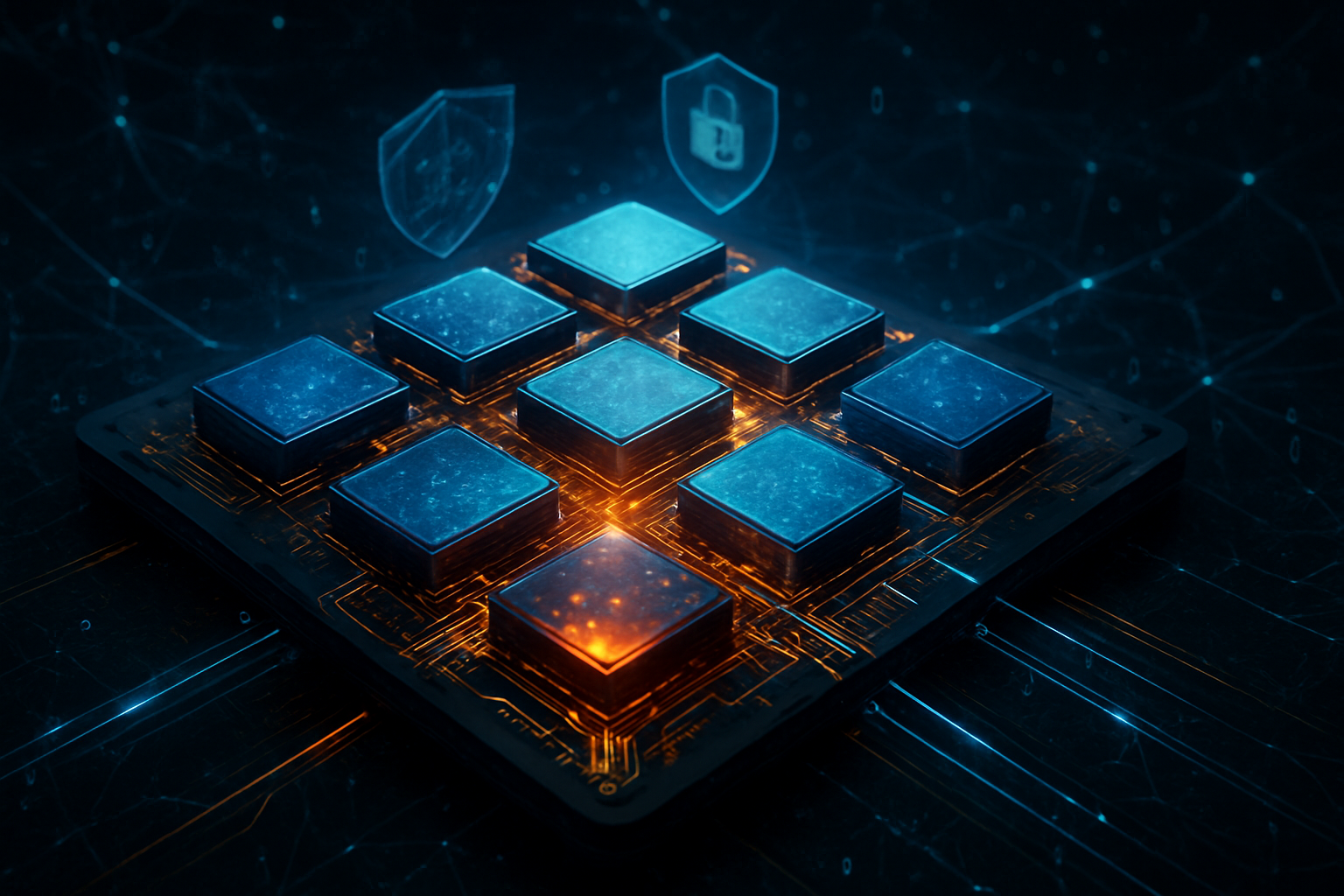
Securing the Multi-Vendor Die: The New Zero-Trust Hardware Frontier
As the industry moves toward a world where a single package contains silicon from multiple different vendors, security has emerged as a paramount concern. You can no longer assume a chip is "trusted" just because it is inside the package. To address this, the industry has adopted a Hierarchical Zero-Trust Architecture. Leveraging the Security Protocol and Data Model (SPDM) 1.3, UCIe-compliant chips now treat every chiplet as a separate entity that must be authenticated. A central "Director" chiplet acts as the Root of Trust (RoT), verifying the identity and integrity of every other "Spoke" chiplet during the boot process through digital certificates and hardware attestation.
Beyond authentication, new protocols have been implemented to mitigate "Trojan chiplets"—malicious hardware hidden in third-party dies. The UCIe DFx Architecture (UDA) provides a dedicated management fabric that monitors telemetry and signal patterns to detect anomalies. Furthermore, to counter side-channel attacks where an attacker might infer cryptographic keys by measuring power or timing signatures, UCIe 3.0 supports "Traffic Padding." This technique ensures constant-time signaling and consistent power draw, effectively hiding sensitive operations from prying neighboring chiplets. These security layers are essential for high-stakes environments like government data centers and autonomous vehicle systems.
Beyond the Reticle Limit: The Future of Heterogeneous AI Integration
Looking toward the late 2020s, the evolution of UCIe is expected to move toward true 3D integration. Experts predict the rise of "memory-on-logic" stacking, where high-bandwidth memory (HBM) is placed directly on top of AI compute cores using hybrid bonding with pitches smaller than one micron. This would virtually eliminate the "memory wall," allowing AI models to scale to sizes previously thought impossible. Additionally, we are seeing the emergence of "self-healing" silicon. With the management capabilities provided by UCIe 3.0, future AI chips will be able to detect a failing chiplet in a stack and dynamically reroute data to healthy components, significantly extending the lifespan of expensive hardware.
The primary challenge remains the thermal management of these dense, stacked structures. Dissipating heat from the middle of a 3D silicon sandwich is a monumental engineering task. However, researchers are already testing integrated liquid cooling channels and new diamond-based heat spreaders to address this. As these hurdles are cleared, we expect the first "Multi-Vendor AI Supercomputer" to emerge, where the CPU, GPU, and NPU are sourced from three different companies and assembled by a fourth, creating a truly open hardware ecosystem for the first time in history.
A Decoupled Future: The Legacy of Universal Connectivity
The emergence of the UCIe standard marks the end of the "monolithic era" and the beginning of a more democratic, efficient, and scalable approach to computing. By breaking the chip apart, the industry has ironically found a way to bring it all together. The ability to mix silicon from diverse vendors ensures that the best-in-class technology can be used for every specific task, rather than being forced into a "jack of all trades, master of none" monolithic design.
As we move through 2026, the industry will be watching for the first large-scale deployments of multi-vendor AI accelerators in data centers. The success of these devices will validate the security and interoperability of the UCIe ecosystem. Ultimately, the move to chiplets represents a shift from "competitive silos" to "collaborative integration," a change that is likely to accelerate AI innovation for decades to come.
This content is intended for informational purposes only and represents analysis of current AI developments.
TokenRing AI delivers enterprise-grade solutions for multi-agent AI workflow orchestration, AI-powered development tools, and seamless remote collaboration platforms.
For more information, visit https://www.tokenring.ai/.