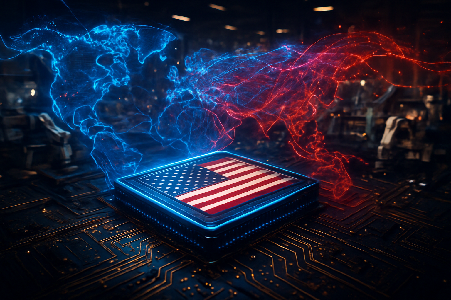
Tag: US Manufacturing

  • TSMC’s Global Gambit: A $165 Billion Bet Reshaping the Semiconductor Landscape in the US and Japan

    TSMC’s Global Gambit: A $165 Billion Bet Reshaping the Semiconductor Landscape in the US and Japan

    Taiwan Semiconductor Manufacturing Company (TSMC) (NYSE: TSM), the world's leading contract chipmaker, is in the midst of an unprecedented global expansion, committing staggering investments totaling $165 billion in the United States and significantly bolstering its presence in Japan. This aggressive diversification strategy is a direct response to escalating geopolitical tensions, particularly between the U.S. and China, the insatiable global demand for advanced semiconductors fueled by the artificial intelligence (AI) boom, and a critical imperative to de-risk and fortify global supply chains. TSMC's strategic moves are not merely about growth; they represent a fundamental reshaping of the semiconductor industry, moving towards a more geographically dispersed and resilient manufacturing ecosystem.

    This monumental undertaking aims to solidify TSMC's position as a "long-term and trustworthy provider of technology and capacity" worldwide. While maintaining its technological vanguard in Taiwan, the company is establishing new production strongholds abroad to mitigate supply chain vulnerabilities, diversify its manufacturing base, and bring production closer to its key global clientele. The scale of this expansion, heavily incentivized by host governments, marks a pivotal moment, shifting the industry away from its concentrated reliance on a single geographic region and heralding a new era of regionalized chip production.

    Unpacking the Gigafab Clusters: A Deep Dive into TSMC's Overseas Manufacturing Prowess

    TSMC's expansion strategy is characterized by massive capital outlays and the deployment of cutting-edge process technologies across its new international hubs. The most significant overseas venture is unfolding in Phoenix, Arizona, where TSMC's commitment has ballooned to an astonishing $165 billion. This includes plans for three advanced fabrication plants (fabs), two advanced packaging facilities, and a major research and development center, making it the largest single foreign direct investment in U.S. history.

    The first Arizona fab (Fab 21) commenced high-volume production of 4-nanometer (N4) process technology in Q4 2024, notably producing wafers for NVIDIA's (NASDAQ: NVDA) Blackwell architecture, crucial for powering the latest AI innovations. Construction of the second fab structure concluded in 2025, with volume production of 3-nanometer (N3) process technology targeted for 2028. Breaking ground in April 2025, the third fab is slated for N2 (2-nanometer) and A16 process technologies, aiming for volume production by the end of the decade. This accelerated timeline, driven by robust AI-related demand from U.S. customers, indicates TSMC's intent to develop an "independent Gigafab cluster" in Arizona, complete with on-site advanced packaging and testing capabilities. This strategic depth aims to create a more complete and resilient semiconductor supply chain ecosystem within the U.S., aligning with the objectives of the CHIPS and Science Act.

    Concurrently, TSMC is bolstering its presence in Japan through Japan Advanced Semiconductor Manufacturing (JASM), a joint venture with Sony (NYSE: SONY) and Denso (TYO: 6902) in Kumamoto. The first Kumamoto facility initiated mass production in late 2024, focusing on more mature process nodes (12 nm, 16 nm, 22 nm, 28 nm), primarily catering to the automotive industry. While plans for a second Kumamoto fab were initially set for Q1 2025, construction has been adjusted to begin in the second half of 2025, with volume production for higher-performance 6nm and 7nm chips, as well as 40nm technology, now expected in the first half of 2029. This slight delay is attributed to local site congestion and a strategic reallocation of resources towards the U.S. fabs. Beyond manufacturing, TSMC is deepening its R&D footprint in Japan, establishing a 3D IC R&D center and a design hub in Osaka, alongside a planned joint research laboratory with the University of Tokyo. This dual approach in both advanced and mature nodes demonstrates a nuanced strategy to diversify capabilities and reduce overall supply chain risks, leveraging strong governmental support and Japan's robust chipmaking infrastructure.

    Reshaping the Tech Ecosystem: Who Benefits and Who Faces New Challenges

    TSMC's global expansion carries profound implications for major AI companies, tech giants, and emerging startups alike, primarily by enhancing supply chain resilience and intensifying competitive dynamics. Companies like NVIDIA, Apple (NASDAQ: AAPL), AMD (NASDAQ: AMD), Broadcom (NASDAQ: AVGO), and Qualcomm (NASDAQ: QCOM), all heavily reliant on TSMC for their cutting-edge chips, stand to gain significant supply chain stability. Localized production in the U.S. means reduced exposure to geopolitical risks and disruptions previously associated with manufacturing concentration in Taiwan. For instance, Apple has committed to sourcing "tens of millions of chips" from the Arizona plant, and NVIDIA's CEO Jensen Huang has publicly acknowledged TSMC's indispensable role, with Blackwell wafers now being produced in the U.S. This proximity allows for closer collaboration and faster iteration on designs, a critical advantage in the rapidly evolving AI landscape.

    The "friendshoring" advantages driven by the U.S. CHIPS Act align TSMC's expansion with national security goals, potentially leading to preferential access and stability for U.S.-based tech companies. Similarly, TSMC's venture in Japan, focusing on mature nodes with partners like Sony and Denso, ensures a stable domestic supply for Japan's vital automotive and electronics sectors. While direct benefits for emerging startups might be less immediate for advanced nodes, the development of robust semiconductor ecosystems around these new facilities—including a skilled workforce, supporting industries, and R&D hubs—can indirectly foster innovation and provide easier access to foundry services.

    However, this expansion also introduces competitive implications and potential disruptions. While solidifying TSMC's dominance, it also fuels regional competition, with other major players like Intel (NASDAQ: INTC) and Samsung (KRX: 005930) also investing heavily in U.S. manufacturing. A significant challenge is the higher production cost; chips produced in the U.S. are estimated to be 30-50% more expensive than those from Taiwan due to labor costs, logistics, and regulatory environments. This could impact the profit margins of some tech companies, though the strategic value of supply chain security often outweighs the cost for critical components. The primary "disruption" is a positive shift towards more robust supply chains, reducing the likelihood of production delays that companies like Apple have experienced. Yet, initial operational delays in Arizona mean that for the absolute bleeding-edge chips, reliance on Taiwan will persist for some time. Ultimately, this expansion leads to a more geographically diversified and resilient semiconductor industry, reshaping market positioning and strategic advantages for all players involved.

    A New Era of Technonationalism: The Wider Significance of TSMC's Global Footprint

    TSMC's global expansion signifies a monumental shift in the broader semiconductor landscape, driven by economic imperatives and escalating geopolitical tensions. This strategic diversification aims to bolster global supply chain resilience while navigating significant challenges related to costs, talent, and maintaining technological parity. This current trajectory marks a notable departure from previous industry milestones, which were primarily characterized by increasing specialization and geographic concentration.

    The concentration of advanced chip production in Taiwan, a potential geopolitical flashpoint, presents an existential risk to the global technology ecosystem. By establishing manufacturing facilities in diverse regions, TSMC aims to mitigate these geopolitical risks, enhance supply chain security, and bring production closer to its major customers. This strategy ensures Taiwan's economic and technological leverage remains intact even amidst shifting geopolitical alliances, while simultaneously addressing national security concerns in the U.S. and Europe, which seek to reduce reliance on foreign chip manufacturing. The U.S. CHIPS Act and similar initiatives in Europe underscore a worldwide effort to onshore semiconductor manufacturing, fostering "chip alliances" where nations provide infrastructure and funding, while TSMC supplies its cutting-edge technology and expertise.

    However, this fragmentation of supply chains is not without concerns. Manufacturing semiconductors outside Taiwan is considerably more expensive, with the cost per wafer in Arizona estimated to be 30-50% higher. While governments are providing substantial subsidies to offset these costs, the long-term profitability and how these extra costs will be transferred to customers remain critical issues. Furthermore, talent acquisition and retention present significant hurdles, with TSMC facing labor shortages and cultural integration challenges in the U.S. While critical production capacity is being diversified, TSMC's most advanced research and development and leading-edge manufacturing (e.g., 2nm and below) are largely expected to remain concentrated in Taiwan, ensuring its "technological supremacy." This expansion represents a reversal of decades of geographic concentration in the semiconductor industry, driven by geopolitics and national security, marking a new era of "technonationalism" and a potential fragmentation of global technology leadership.

    The Road Ahead: Future Developments and Expert Predictions

    Looking ahead, TSMC's global expansion is poised for significant near-term and long-term developments, with the U.S. and Japan operations playing pivotal roles in the company's strategic roadmap. In the United States, TSMC is accelerating its plans to establish a "gigafab" cluster in Arizona, aiming to eventually handle around 30% of its most advanced chip production, encompassing 2nm and more cutting-edge A16 process technologies. The total investment is projected to reach $165 billion, with a strategic goal of completing a domestic AI supply chain through the addition of advanced packaging facilities. This long-term strategy aims to create a self-contained pathway for U.S. customers, reducing the need to send work back to Taiwan for final assembly.

    In Japan, beyond the second Kumamoto fab, there is potential for TSMC to consider a third plant, signaling Japan's ambition to become a significant semiconductor production hub. TSMC is also exploring the possibility of shifting parts of its advanced packaging capabilities, 3DFabric, closer to Japan as demand grows. This move would further bolster Japan's efforts to revive its semiconductor manufacturing capabilities and establish the country as a center for semiconductor research and development. The expanded production capacity in both regions is set to serve a broad range of high-demand applications, with artificial intelligence (AI) being a primary driver, alongside high-performance computing (HPC), the automotive industry, 5G, and next-generation communication systems.

    However, several key challenges persist. Higher operating costs in the U.S. are expected to lead to a temporary decline in TSMC's gross margins. Labor shortages and talent acquisition remain significant hurdles in both the U.S. and Japan, compounded by infrastructure issues and slower permitting processes in some regions. Geopolitical risks and trade policies continue to influence investment calculations, alongside concerns about potential overcapacity and the long-term sustainability of government subsidies. Industry experts predict that the Arizona fabs will become a cornerstone of TSMC's global roadmap, with significant production of 2nm and beyond chips by the end of the decade, aligning with the U.S.'s goal of increased semiconductor self-sufficiency. In Japan, TSMC's presence is expected to foster closer cooperation with local integrated device manufacturers and system integrators, significantly supporting market expansion in the automotive chip sector. While overseas expansion is crucial for strategic diversification, TSMC's CFO Wendell Huang has projected short-term financial impacts, though the long-term strategic benefits and robust AI demand are expected to offset these near-term costs.

    A Defining Moment in Semiconductor History: The Long-Term Impact

    TSMC's audacious global expansion, particularly its monumental investments in the United States and Japan, represents a defining moment in the history of the semiconductor industry. The key takeaway is a fundamental shift from a hyper-concentrated, efficiency-driven global supply chain to a more diversified, resilience-focused, and geopolitically influenced manufacturing landscape. This strategy is not merely about corporate growth; it is an assessment of the development's significance in safeguarding the foundational technology of the modern world against an increasingly volatile global environment.

    The long-term impact will see a more robust and secure global semiconductor supply chain, albeit potentially at a higher cost. The establishment of advanced manufacturing hubs outside Taiwan will reduce the industry's vulnerability to regional disruptions, natural disasters, or geopolitical conflicts. This decentralization will foster stronger regional ecosystems, creating thousands of high-tech jobs and stimulating significant indirect economic growth in host countries. What to watch for in the coming weeks and months includes further updates on construction timelines, particularly for the second and third Arizona fabs and the second Kumamoto fab, and how TSMC navigates the challenges of talent acquisition and cost management in these new regions. The ongoing dialogue between governments and industry leaders regarding subsidies, trade policies, and technological collaboration will also be crucial in shaping the future trajectory of this global semiconductor rebalancing act. This strategic pivot by TSMC is a testament to the critical role semiconductors play in national security and economic prosperity, setting a new precedent for global technological leadership.


    This content is intended for informational purposes only and represents analysis of current AI developments.

    TokenRing AI delivers enterprise-grade solutions for multi-agent AI workflow orchestration, AI-powered development tools, and seamless remote collaboration platforms.
    For more information, visit https://www.tokenring.ai/.

  • America’s Power Play: GaN Chips and the Resurgence of US Manufacturing

    America’s Power Play: GaN Chips and the Resurgence of US Manufacturing

    The United States is experiencing a pivotal moment in its technological landscape, marked by a significant and accelerating trend towards domestic manufacturing of power chips. This strategic pivot, heavily influenced by government initiatives and substantial private investment, is particularly focused on advanced materials like Gallium Nitride (GaN). As of late 2025, this movement holds profound implications for national security, economic leadership, and the resilience of critical supply chains, directly addressing vulnerabilities exposed by recent global disruptions.

    At the forefront of this domestic resurgence is GlobalFoundries (NASDAQ: GFS), a leading US-based contract semiconductor manufacturer. Through strategic investments, facility expansions, and key technology licensing agreements—most notably a recent partnership with Taiwan Semiconductor Manufacturing Company (NYSE: TSM) for GaN technology—GlobalFoundries is cementing its role in bringing cutting-edge power chip production back to American soil. This concerted effort is not merely about manufacturing; it's about securing the foundational components for the next generation of artificial intelligence, electric vehicles, and advanced defense systems, ensuring that the US remains a global leader in critical technological innovation.

    GaN Technology: Fueling the Next Generation of Power Electronics

    The shift towards GaN power chips represents a fundamental technological leap from traditional silicon-based semiconductors. As silicon CMOS technologies approach their physical and performance limits, GaN emerges as a superior alternative, offering a host of advantages that are critical for high-performance and energy-efficient applications. Its inherent material properties allow GaN devices to operate at significantly higher voltages, frequencies, and temperatures with vastly reduced energy loss compared to their silicon counterparts.

    Technically, GaN's wide bandgap and high electron mobility enable faster switching speeds and lower on-resistance, translating directly into greater energy efficiency and reduced heat generation. This superior performance allows for the design of smaller, lighter, and more compact electronic components, a crucial factor in space-constrained applications ranging from consumer electronics to electric vehicle powertrains and aerospace systems. This departure from previous silicon-centric approaches is not merely an incremental improvement but a foundational change, promising increased power density and overall system miniaturization. The semiconductor industry, including leading research institutions and industry experts, has reacted with widespread enthusiasm, recognizing GaN as a critical enabler for future technological advancements, particularly in power management and RF applications.

    GlobalFoundries' recent strategic moves underscore the importance of GaN. On November 10, 2025, GlobalFoundries announced a significant technology licensing agreement with TSMC for 650V and 80V GaN technology. This partnership is designed to accelerate GF’s development and US-based production of next-generation GaN power chips. The licensed technology will be qualified at GF's Burlington, Vermont facility, leveraging its existing expertise in high-voltage GaN-on-Silicon. Development is slated for early 2026, with production ramping up later that year, making products available by late 2026. This move positions GF to provide a robust, US-based GaN supply chain for a global customer base, distinguishing it from fabs primarily located in Asia.

    Competitive Implications and Market Positioning in the AI Era

    The growing emphasis on US-based GaN power chip manufacturing carries significant implications for a diverse range of companies, from established tech giants to burgeoning AI startups. Companies heavily invested in power-intensive technologies stand to benefit immensely from a secure, domestic supply of high-performance GaN chips. Electric vehicle manufacturers, for instance, will find more robust and efficient solutions for powertrains, on-board chargers, and inverters, potentially accelerating the development of next-generation EVs. Similarly, data center operators, constantly seeking to reduce energy consumption and improve efficiency, will leverage GaN-based power supplies to minimize operational costs and environmental impact.

    For major AI labs and tech companies, the availability of advanced GaN power chips manufactured domestically translates into enhanced supply chain security and reduced geopolitical risks, crucial for maintaining uninterrupted research and development cycles. Companies like Apple (NASDAQ: AAPL), SpaceX, AMD (NASDAQ: AMD), Qualcomm Technologies (NASDAQ: QCOM), NXP (NASDAQ: NXPI), and GM (NYSE: GM) are already committing to reshoring semiconductor production and diversifying their supply chains, directly benefiting from GlobalFoundries' expanded capabilities. This trend could disrupt existing product roadmaps that relied heavily on overseas manufacturing, potentially shifting competitive advantages towards companies with strong domestic partnerships.

    In terms of market positioning, GlobalFoundries is strategically placing itself as a critical enabler for the future of power electronics. By focusing on differentiated GaN-based power capabilities in Vermont and investing $16 billion across its New York and Vermont facilities, GF is not just expanding capacity but also accelerating growth in AI-enabling and power-efficient technologies. This provides a strategic advantage for customers seeking secure, high-performance power devices manufactured in the United States, thereby fostering a more resilient and geographically diverse semiconductor ecosystem. The ability to source critical components domestically will become an increasingly valuable differentiator in a competitive global market, offering both supply chain stability and potential intellectual property protection.

    Broader Significance: Reshaping the Global Semiconductor Landscape

    The resurgence of US-based GaN power chip manufacturing represents a critical inflection point in the broader AI and semiconductor landscape, signaling a profound shift towards greater supply chain autonomy and technological sovereignty. This initiative directly addresses the geopolitical vulnerabilities exposed by the global reliance on a concentrated few regions for advanced chip production, particularly in East Asia. The CHIPS and Science Act, with its substantial funding and strategic guardrails, is not merely an economic stimulus but a national security imperative, aiming to re-establish the United States as a dominant force in semiconductor innovation and production.

    The impacts of this trend are multifaceted. Economically, it promises to create high-skilled jobs, stimulate regional economies, and foster a robust ecosystem of research and development within the US. Technologically, the domestic production of advanced GaN chips will accelerate innovation in critical sectors such as AI, 5G/6G communications, defense systems, and renewable energy, where power efficiency and performance are paramount. This move also mitigates potential concerns around intellectual property theft and ensures a secure supply of components vital for national defense infrastructure. Comparisons to previous AI milestones reveal a similar pattern of foundational technological advancements driving subsequent waves of innovation; just as breakthroughs in processor design fueled early AI, secure and advanced power management will be crucial for scaling future AI capabilities.

    The strategic importance of this movement cannot be overstated. By diversifying its semiconductor manufacturing base, the US is building resilience against future geopolitical disruptions, natural disasters, or pandemics that could cripple global supply chains. Furthermore, the focus on GaN, a technology critical for high-performance computing and energy efficiency, positions the US to lead in the development of greener, more powerful AI systems and sustainable infrastructure. This is not just about manufacturing chips; it's about laying the groundwork for sustained technological leadership and safeguarding national interests in an increasingly interconnected and competitive world.

    Future Developments: The Road Ahead for GaN and US Manufacturing

    The trajectory for US-based GaN power chip manufacturing points towards significant near-term and long-term developments. In the immediate future, the qualification of TSMC-licensed GaN technology at GlobalFoundries' Vermont facility, with production expected to commence in late 2026, will mark a critical milestone. This will rapidly increase the availability of domestically produced, advanced GaN devices, serving a global customer base. We can anticipate further government incentives and private investments flowing into research and development, aiming to push the boundaries of GaN technology even further, exploring higher voltage capabilities, improved reliability, and integration with other advanced materials.

    On the horizon, potential applications and use cases are vast and transformative. Beyond current applications in EVs, data centers, and 5G infrastructure, GaN chips are expected to play a crucial role in next-generation aerospace and defense systems, advanced robotics, and even in novel energy harvesting and storage solutions. The increased power density and efficiency offered by GaN will enable smaller, lighter, and more powerful devices, fostering innovation across numerous industries. Experts predict a continued acceleration in the adoption of GaN, especially as manufacturing costs decrease with economies of scale and as the technology matures further.

    However, challenges remain. Scaling production to meet burgeoning demand, particularly for highly specialized GaN-on-silicon wafers, will require sustained investment in infrastructure and a skilled workforce. Research into new GaN device architectures and packaging solutions will be essential to unlock its full potential. Furthermore, ensuring that the US maintains its competitive edge in GaN innovation against global rivals will necessitate continuous R&D funding and strategic collaborations between industry, academia, and government. The coming years will see a concerted effort to overcome these hurdles, solidifying the US position in this critical technology.

    Comprehensive Wrap-up: A New Dawn for American Chipmaking

    The strategic pivot towards US-based manufacturing of advanced power chips, particularly those leveraging Gallium Nitride technology, represents a monumental shift in the global semiconductor landscape. Key takeaways include the critical role of government initiatives like the CHIPS and Science Act in catalyzing domestic investment, the superior performance and efficiency of GaN over traditional silicon, and the pivotal leadership of companies like GlobalFoundries in establishing a robust domestic supply chain. This development is not merely an economic endeavor but a national security imperative, aimed at fortifying critical infrastructure and maintaining technological sovereignty.

    This movement's significance in AI history is profound, as secure and high-performance power management is foundational for the continued advancement and scaling of artificial intelligence systems. The ability to domestically produce the energy-efficient components that power everything from data centers to autonomous vehicles will directly influence the pace and direction of AI innovation. The long-term impact will be a more resilient, geographically diverse, and technologically advanced semiconductor ecosystem, less vulnerable to external disruptions and better positioned to drive future innovation.

    In the coming weeks and months, industry watchers should closely monitor the progress at GlobalFoundries' Vermont facility, particularly the qualification and ramp-up of the newly licensed GaN technology. Further announcements regarding partnerships, government funding allocations, and advancements in GaN research will provide crucial insights into the accelerating pace of this transformation. The ongoing commitment to US-based manufacturing of power chips signals a new dawn for American chipmaking, promising a future of enhanced security, innovation, and economic leadership.


    This content is intended for informational purposes only and represents analysis of current AI developments.

    TokenRing AI delivers enterprise-grade solutions for multi-agent AI workflow orchestration, AI-powered development tools, and seamless remote collaboration platforms.
    For more information, visit https://www.tokenring.ai/.

  • GlobalFoundries and TSMC Forge Landmark GaN Alliance, Reshaping US Power Chip Manufacturing

    GlobalFoundries and TSMC Forge Landmark GaN Alliance, Reshaping US Power Chip Manufacturing

    In a pivotal development set to redefine the landscape of power semiconductor manufacturing, GlobalFoundries (NASDAQ: GFS) announced on November 10, 2025, a significant technology licensing agreement with Taiwan Semiconductor Manufacturing Company (NYSE: TSM). This strategic partnership focuses on advanced Gallium Nitride (GaN) technology, specifically 650V and 80V platforms, and is poised to dramatically accelerate GlobalFoundries' development and U.S.-based production of next-generation GaN power chips. The immediate significance lies in fortifying the domestic supply chain for critical power components, addressing burgeoning demand across high-growth sectors.

    This collaboration emerges at a crucial juncture, as TSMC, a global foundry leader, prepares to strategically exit its broader GaN foundry services by July 2027 to intensify its focus on advanced-node silicon for AI applications and advanced packaging. GlobalFoundries' acquisition of this proven GaN expertise not only ensures the continued availability and advancement of the technology but also strategically positions its Burlington, Vermont, facility as a vital hub for U.S.-manufactured GaN semiconductors, bolstering national efforts towards semiconductor independence and resilience.

    Technical Prowess: Unpacking the Advanced GaN Technology

    The licensed technology from TSMC encompasses both 650V and 80V GaN-on-Silicon (GaN-on-Si) capabilities. GlobalFoundries will leverage its existing high-voltage GaN-on-Silicon expertise at its Burlington facility to integrate and scale this technology, with a strong focus on 200mm (8-inch) wafer manufacturing for high-volume production. This move is particularly impactful as TSMC had previously developed robust second-generation GaN-on-Si processes, and GlobalFoundries is now gaining access to this established and validated technology.

    GaN technology offers substantial performance advantages over traditional silicon-based semiconductors in power applications due to its wider bandgap. Key differentiators include significantly higher energy efficiency and power density, enabling smaller, more compact designs. GaN devices boast faster switching speeds—up to 10 times faster than silicon MOSFETs and 100 times faster than IGBTs—which allows for higher operating frequencies and smaller passive components. Furthermore, GaN exhibits superior thermal performance, efficiently dissipating heat and reducing the need for complex cooling systems.

    Unlike previous approaches that relied heavily on silicon, which is reaching its performance limits in terms of efficiency and power density, GaN provides a critical leap forward. While Silicon Carbide (SiC) is another wide bandgap material, GaN-on-Silicon offers a cost-effective solution for operating voltages below 1000V by utilizing existing silicon manufacturing infrastructure. Initial reactions from the semiconductor research community and industry experts have been largely positive, viewing this as a strategic win for GlobalFoundries and a significant step towards strengthening the U.S. domestic semiconductor ecosystem, especially given TSMC's strategic pivot.

    The technology is targeted for high-performance, energy-efficient applications across various sectors, including power management solutions for data centers, industrial power applications, and critical components for electric vehicles (EVs) such as onboard chargers and DC-DC converters. It also holds promise for renewable energy systems, fast-charging electronics, IoT devices, and even aerospace and defense applications requiring robust RF and high-power control. GlobalFoundries emphasizes a holistic approach to GaN reliability, designing for harsh environments to ensure robustness and longevity.

    Market Ripple Effects: Impact on the Semiconductor Industry

    This strategic partnership carries profound implications for semiconductor companies, tech giants, and startups alike. GlobalFoundries (NASDAQ: GFS) stands as the primary beneficiary, gaining rapid access to proven GaN technology that will significantly accelerate its GaN roadmap and bolster its position as a leading contract manufacturer. This move allows GF to address the growing demand for higher efficiency and power density in power systems, offering a crucial U.S.-based manufacturing option for GaN-on-silicon semiconductors.

    For other semiconductor companies, the landscape is shifting. Companies that previously relied on TSMC (NYSE: TSM) for GaN foundry services, such as Navitas Semiconductor (NASDAQ: NVTS) and ROHM (TSE: 6963), have already begun seeking alternative manufacturing partners due to TSMC's impending exit. GlobalFoundries, with its newly acquired technology and planned U.S. production, is now poised to become a key alternative foundry, potentially capturing a significant portion of this reallocated business. This intensifies competition for established players like Infineon Technologies (OTC: IFNNY) and Innoscience, which are also major forces in the power semiconductor and GaN markets.

    Tech giants involved in cloud computing, electric vehicles, and advanced industrial equipment stand to benefit from a more diversified and robust GaN supply chain. The increased manufacturing capacity and technological expertise at GlobalFoundries will lead to a wider availability of GaN power devices, enabling these companies to integrate more energy-efficient and compact designs into their products. For startups focused on innovative GaN-based power management solutions, GlobalFoundries' entry provides a reliable manufacturing partner, potentially lowering barriers to entry and accelerating time-to-market.

    The primary disruption stems from TSMC's withdrawal from GaN foundry services, which necessitates a transition for its current GaN customers. However, GlobalFoundries' timely entry with licensed TSMC technology can mitigate some of this disruption by offering a familiar and proven process. This development significantly bolsters U.S.-based manufacturing capabilities for advanced semiconductors, enhancing market positioning and strategic advantages for GlobalFoundries by offering U.S.-based GaN capacity to a global customer base, aligning with national initiatives to strengthen domestic chip production.

    Broader Significance: A New Era for Power Electronics

    The GlobalFoundries and TSMC GaN technology licensing agreement signifies a critical juncture in the broader semiconductor manufacturing landscape, underscoring a decisive shift towards advanced materials and enhanced supply chain resilience. This partnership accelerates the adoption of GaN, a "third-generation" semiconductor material, which offers superior performance characteristics over traditional silicon, particularly in high-power and high-frequency applications. Its ability to deliver higher efficiency, faster switching speeds, and better thermal management is crucial as silicon-based CMOS technologies approach their fundamental limits.

    This move fits perfectly into current trends driven by the surging demand from next-generation technologies such as 5G telecommunications, electric vehicles, data centers, and renewable energy systems. The market for GaN semiconductor devices is projected for substantial growth, with some estimates predicting the power GaN market to reach approximately $3 billion by 2030. The agreement's emphasis on establishing U.S.-based GaN capacity directly addresses pressing concerns about supply chain resilience, especially given the geopolitical sensitivity surrounding raw materials like gallium. Diversifying manufacturing locations for critical components is a top priority for national security and economic stability.

    The impacts on global chip production are multifaceted. It promises increased availability and competition in the GaN market, offering customers an additional U.S.-based manufacturing option that could reduce lead times and geopolitical risks. This expanded capacity will enable more widespread integration of GaN into new product designs across various industries, leading to more efficient and compact electronic systems. While intellectual property (IP) is always a concern in such agreements, the history of cross-licensing and cooperation between TSMC and GlobalFoundries suggests a framework for managing such issues, allowing both companies freedom to operate and innovate.

    Comparisons to previous semiconductor industry milestones are apt. This shift from silicon to GaN for specific applications mirrors the earlier transition from germanium to silicon in the early days of transistors, driven by superior material properties. It represents a "vertical" advancement in material capability, distinct from the "horizontal" scaling achieved through lithography advancements, promising to enable new generations of power-efficient devices. This strategic collaboration also highlights the industry's evolving approach to IP, where licensing agreements facilitate technological progress rather than being bogged down by disputes.

    The Road Ahead: Future Developments and Challenges

    The GlobalFoundries and TSMC GaN partnership heralds significant near-term and long-term developments for advanced GaN power chips. In the near term, development of the licensed technology is slated to commence in early 2026 at GlobalFoundries' Burlington, Vermont facility, with initial production expected to ramp up later that year. This rapid integration aims to quickly bring high-performance GaN solutions to market, leveraging GlobalFoundries' existing expertise and significant federal funding (over $80 million since 2020) dedicated to advancing GaN-on-silicon manufacturing in the U.S.

    Long-term, the partnership is set to deliver GaN chips that will address critical power gaps across mission-critical applications in data centers, automotive, and industrial sectors. The comprehensive GaN portfolio GlobalFoundries is developing, designed for harsh environments and emphasizing reliability, will solidify GaN's role as a next-generation solution for achieving higher efficiency, power density, and compactness where traditional silicon CMOS technologies approach their limits.

    Potential applications and use cases for these advanced GaN power chips are vast and transformative. In Artificial Intelligence (AI), GaN is crucial for meeting the exponential energy demands of AI data centers, enabling power supplies to evolve for higher computational power within reduced footprints. For Electric Vehicles (EVs), GaN promises extended range and faster charging capabilities through smaller, lighter, and more efficient power conversion systems in onboard chargers and DC-DC converters, with future potential in traction inverters. In Renewable Energy, GaN will enhance energy conversion efficiency in solar inverters, wind turbine systems, and overall grid infrastructure, contributing to grid stability and decarbonization efforts.

    Despite its promising future, GaN technology faces challenges, particularly concerning U.S.-based manufacturing capabilities. These include the higher initial cost of GaN components, the complexities of manufacturing scalability and yield (such as lattice mismatch defects when growing GaN on silicon), and ensuring long-term reliability in harsh operating environments. A critical challenge for the U.S. is the current lack of sufficient domestic epitaxy capacity, a crucial step in GaN production, necessitating increased investment to secure the supply chain.

    Experts predict a rapid expansion of the GaN market, with significant growth projected through 2030 and beyond, driven by AI and electrification. GaN is expected to displace legacy silicon in many high-power applications, becoming ubiquitous in power conversion stages from consumer devices to grid-scale energy storage. Future innovations will focus on increased integration, with GaN power FETs combined with control, drive, sensing, and protection circuitry into single, high-performance GaN ICs. The transition to larger wafer sizes (300mm) and advancements in vertical GaN technology are also anticipated to further enhance efficiency and cost-effectiveness.

    A New Chapter in US Chip Independence

    The GlobalFoundries and TSMC GaN technology licensing agreement marks a monumental step, not just for the companies involved, but for the entire semiconductor industry and the broader global economy. The key takeaway is the strategic acceleration of U.S.-based GaN manufacturing, driven by a world-class technology transfer. This development is profoundly significant in the context of semiconductor manufacturing history, representing a critical shift towards advanced materials and a proactive approach to supply chain resilience.

    Its long-term impact on U.S. chip independence and technological advancement is substantial. By establishing a robust domestic hub for advanced GaN production at GlobalFoundries' Vermont facility, the U.S. gains greater control over the manufacturing of essential components for strategic sectors like defense, electric vehicles, and renewable energy. This not only enhances national security but also fosters innovation within the U.S. semiconductor ecosystem, driving economic growth and creating high-tech jobs.

    In the coming weeks and months, industry observers and consumers should closely watch for GlobalFoundries' qualification and production milestones at its Vermont facility in early 2026, followed by the availability of initial products later that year. Monitor customer adoption and design wins, particularly in the data center, industrial, and automotive sectors, as these will be crucial indicators of market acceptance. Keep an eye on the evolving GaN market pricing and competition, especially with TSMC's exit and the continued pressure from other global players. Finally, continued U.S. government support and broader technological advancements in GaN, such as larger wafer sizes and new integration techniques, will be vital to watch for as this partnership unfolds and shapes the future of power electronics.


    This content is intended for informational purposes only and represents analysis of current AI developments.

    TokenRing AI delivers enterprise-grade solutions for multi-agent AI workflow orchestration, AI-powered development tools, and seamless remote collaboration platforms.
    For more information, visit https://www.tokenring.ai/.

  • Nvidia’s Arizona Gambit: Forging America’s AI Future with Domestic Chip Production

    Nvidia’s Arizona Gambit: Forging America’s AI Future with Domestic Chip Production

    Nvidia's (NASDAQ: NVDA) strategic pivot towards localizing the production of its cutting-edge artificial intelligence (AI) chips within the United States, particularly through significant investments in Arizona, marks a watershed moment in the global technology landscape. This bold initiative, driven by a confluence of surging AI demand, national security imperatives, and a push for supply chain resilience, aims to solidify America's leadership in the AI era. The immediate significance of this move is profound, establishing a robust domestic infrastructure for the "engines of the world's AI," thereby mitigating geopolitical risks and fostering an accelerated pace of innovation on U.S. soil.

    This strategic shift is a direct response to global calls for re-industrialization and a reduction in reliance on concentrated overseas manufacturing. By bringing the production of its most advanced AI processors, including the powerful Blackwell architecture, to U.S. facilities, Nvidia is not merely expanding its manufacturing footprint but actively reshaping the future of AI development and the stability of the critical AI chip supply chain. This commitment, underscored by substantial financial investment and extensive partnerships, positions the U.S. at the forefront of the burgeoning AI industrial revolution.

    Engineering the Future: Blackwell Chips and the Arizona Production Hub

    Nvidia's most powerful AI chip architecture, Blackwell, is now in full volume production at Taiwan Semiconductor Manufacturing Company's (NYSE: TSM) facilities in Phoenix, Arizona. This represents a historic departure from manufacturing these cutting-edge chips exclusively in Taiwan, with Nvidia CEO Jensen Huang heralding it as the first time the "engines of the world's AI infrastructure are being built in the United States." This advanced production leverages TSMC's capabilities to produce sophisticated 4-nanometer and 5-nanometer chips, with plans to advance to 3-nanometer, 2-nanometer, and even A16 technologies in the coming years.

    The Blackwell architecture itself is a marvel of engineering, with flagship products like the Blackwell Ultra designed to deliver up to 15 petaflops of performance for demanding AI workloads, each chip packing an astonishing 208 billion transistors. These chips feature an enhanced Transformer Engine optimized for large language models and a new Decompression Engine to accelerate database queries, representing a significant leap over their Hopper predecessors. Beyond wafer fabrication, Nvidia has forged critical partnerships for advanced packaging and testing operations in Arizona with companies like Amkor (NASDAQ: AMKR) and SPIL, utilizing complex chip-on-wafer-on-substrate (CoWoS) technology, specifically CoWoS-L, for its Blackwell chips.

    This approach differs significantly from previous strategies that heavily relied on a centralized, often overseas, manufacturing model. By diversifying its supply chain and establishing an integrated U.S. ecosystem—from fabrication in Arizona to packaging and testing in Arizona, and supercomputer assembly in Texas with partners like Foxconn (TWSE: 2317) and Wistron (TWSE: 3231)—Nvidia is building a more resilient and secure supply chain. While initial fabrication is moving to the U.S., a crucial aspect of high-end AI chip production, advanced packaging, still largely depends on facilities in Taiwan, though Amkor's upcoming Arizona plant by 2027-2028 aims to localize this critical process.

    Initial reactions from the AI research community and industry experts have been overwhelmingly positive, viewing Nvidia's technical pivot to U.S. production as a crucial step towards a more robust and secure AI infrastructure. Experts commend the move for strengthening the U.S. semiconductor supply chain and securing America's leadership in artificial intelligence, acknowledging the strategic importance of mitigating geopolitical risks. While acknowledging the higher manufacturing costs in the U.S. compared to Taiwan, the national security and supply chain benefits are widely considered paramount.

    Reshaping the AI Ecosystem: Implications for Companies and Competitive Dynamics

    Nvidia's aggressive push for AI chip production in the U.S. is poised to significantly reshape the competitive landscape for AI companies, tech giants, and startups. Domestically, U.S.-based AI labs, cloud providers, and startups stand to benefit immensely from faster and more reliable access to Nvidia's cutting-edge hardware. This localized supply chain can accelerate innovation cycles, reduce lead times, and provide a strategic advantage in developing and deploying next-generation AI solutions. Major American tech giants like Google (NASDAQ: GOOGL), Microsoft (NASDAQ: MSFT), Meta (NASDAQ: META), and Oracle (NYSE: ORCL), all significant customers of Nvidia's advanced chips, will benefit from enhanced supply chain resilience and potentially quicker access to the foundational hardware powering their vast AI initiatives.

    However, the implications extend beyond domestic advantages. Nvidia's U.S. production strategy, coupled with export restrictions on its most advanced chips to certain regions like China, creates a growing disparity in AI computing power globally. Non-U.S. companies in restricted regions may face significant limitations in acquiring top-tier Nvidia hardware, compelling them to invest more heavily in indigenous chip development or seek alternative suppliers. This could lead to a fragmented global AI landscape, where access to the most advanced hardware becomes a strategic national asset.

    The move also has potential disruptive effects on existing products and services. While it significantly strengthens supply chain resilience, the higher manufacturing costs in the U.S. could translate to increased prices for AI infrastructure and services, potentially impacting profit margins or being passed on to end-users. Conversely, the accelerated AI innovation within the U.S. due to enhanced hardware access could lead to the faster development and deployment of new AI products and services by American companies, potentially disrupting global market dynamics and establishing new industry standards.

    Nvidia's market positioning is further solidified by this strategy. It is positioning itself not just as a chip supplier but as a critical infrastructure partner for governments and major industries. By securing a domestic supply of its most advanced AI chips, Nvidia reinforces its technological leadership and aligns with U.S. policy goals of re-industrializing and maintaining a technological edge. This enhanced control over the domestic "AI technology stack" provides a unique competitive advantage, enabling closer integration and optimization of hardware and software, and propelling Nvidia's market valuation to an unprecedented $5 trillion.

    A New Industrial Revolution: Wider Significance and Geopolitical Chess

    Nvidia's U.S. AI chip production strategy is not merely an expansion of manufacturing; it's a foundational element of the broader AI landscape and an indicator of significant global trends. These chips are the "engines" powering the generative AI revolution, large language models, high-performance computing, robotics, and autonomous systems across every conceivable industry. The establishment of "AI factories"—data centers specifically designed for AI processing—underscores the profound shift towards AI as a core industrial infrastructure, driving what many are calling a new industrial revolution.

    The economic impacts are projected to be immense. Nvidia's commitment to produce up to $500 billion in AI infrastructure in the U.S. over the next four years is expected to create hundreds of thousands, if not millions, of high-quality jobs and generate trillions of dollars in economic activity. This strengthens the U.S. semiconductor industry and ensures its capacity to meet the surging global demand for AI technologies, reinforcing the "Made in America" agenda.

    Geopolitically, this move is a strategic chess piece. It aims to enhance supply chain resilience and reduce reliance on Asian production, particularly Taiwan, amidst escalating trade tensions and the ongoing technological rivalry with China. U.S. government incentives, such as the CHIPS and Science Act, and direct pressure have influenced this shift, with the goal of maintaining American technological dominance. However, U.S. export controls on advanced AI chips to China have created a complex "AI Cold War," impacting Nvidia's revenue from the Chinese market and intensifying the global race for AI supremacy.

    Potential concerns include the higher cost of manufacturing in the U.S., though Nvidia anticipates improved efficiency over time. More broadly, Nvidia's near-monopoly in high-performance AI chips has raised concerns about market concentration and potential anti-competitive practices, leading to antitrust scrutiny. The U.S. policy of reserving advanced AI chips for American companies and allies, while limiting access for rivals, also raises questions about global equity in AI development and could exacerbate the technological divide. This era is often compared to a new "industrial revolution," with Nvidia's rise built on decades of foresight in recognizing the power of GPUs for parallel computing, a bet that now underpins the pervasive industrial and economic integration of AI.

    The Road Ahead: Future Developments and Expert Predictions

    Nvidia's strategic expansion in the U.S. is a long-term commitment. In the near term, the focus will be on the full ramp-up of Blackwell chip production in Arizona and the operationalization of AI supercomputer manufacturing plants in Texas, with mass production expected in the next 12-15 months. Nvidia also unveiled its next-generation AI chip, "Vera Rubin" (or "Rubin"), at the GTC conference in October 2025, with Rubin GPUs slated for mass production in late 2026. This continuous innovation in chip architecture, coupled with localized production, will further cement the U.S.'s role as a hub for advanced AI hardware.

    These U.S.-produced AI chips and supercomputers are poised to be the "engines" for a new era of "AI factories," driving an "industrial revolution" across every sector. Potential applications include accelerating machine learning and deep learning processes, revolutionizing big data analytics, boosting AI capabilities in edge devices, and enabling the development of "physical AI" through digital twins and advanced robotics. Nvidia's partnerships with robotics companies like Figure also highlight its commitment to advancing next-generation humanoid robotics.

    However, significant challenges remain. The higher cost of domestic manufacturing is a persistent concern, though Nvidia views it as a necessary investment for national security and supply chain resilience. A crucial challenge is addressing the skilled labor shortage in advanced semiconductor manufacturing, packaging, and testing, even with Nvidia's plans for automation and robotics. Geopolitical shifts and export controls, particularly concerning China, continue to pose significant hurdles, with the U.S. government's stringent restrictions prompting Nvidia to develop region-specific products and navigate a complex regulatory landscape. Experts predict that these restrictions will compel China to further accelerate its indigenous AI chip development.

    Experts foresee that Nvidia's strategy will create hundreds of thousands, potentially millions, of high-quality jobs and drive trillions of dollars in economic security in the U.S. The decision to keep the most powerful AI chips primarily within the U.S. is seen as a pivotal moment for national competitive strength in AI. Nvidia is expected to continue its strategy of deep vertical integration, co-designing hardware and software across the entire stack, and expanding into areas like quantum computing and advanced telecommunications. Industry leaders also urge policymakers to strike a balance with export controls to safeguard national security without stifling innovation.

    A Defining Era: Wrap-Up and What to Watch For

    Nvidia's transformative strategy for AI chip production in the United States, particularly its deep engagement in Arizona, represents a historic milestone in U.S. manufacturing and a defining moment in AI history. By bringing the fabrication of its most advanced Blackwell AI chips to TSMC's facilities in Phoenix and establishing a comprehensive domestic ecosystem for supercomputer assembly and advanced packaging, Nvidia is actively re-industrializing the nation and fortifying its critical AI supply chain. The company's commitment of up to $500 billion in U.S. AI infrastructure underscores the profound economic and strategic benefits anticipated, including massive job creation and trillions in economic security.

    This development signifies a robust comeback for America in advanced semiconductor fabrication, cementing its role as a preeminent force in AI hardware development and significantly reducing reliance on Asian manufacturing amidst escalating geopolitical tensions. The U.S. government's proactive stance in prioritizing domestic production, coupled with policies to reserve advanced chips for American companies, carries profound national security implications, aiming to safeguard technological leadership in what is increasingly being termed the "AI industrial revolution."

    In the long term, this strategy is expected to yield substantial economic and strategic advantages for the U.S., accelerating AI innovation and infrastructure development domestically. However, the path forward is not without challenges, including the higher costs of U.S. manufacturing, the imperative to cultivate a skilled workforce, and the complex geopolitical landscape shaped by export restrictions and technological rivalries, particularly with China. The fragmentation of global supply chains and the intensification of the race for technological sovereignty will be defining features of this era.

    In the coming weeks and months, several key developments warrant close attention. Watch for further clarifications from the Commerce Department regarding "advanced" versus "downgraded" chip definitions, which will dictate global access to Nvidia's products. The operational ramp-up of Nvidia's supercomputer manufacturing plants in Texas will be a significant indicator of progress. Crucially, the completion and operationalization of Amkor's $2 billion packaging facility in Arizona by 2027-2028 will be pivotal, enabling full CoWoS packaging capabilities in the U.S. and further reducing reliance on Taiwan. The evolving competitive landscape, with other tech giants pursuing their own AI chip designs, and the broader geopolitical implications of these protectionist measures on international trade will continue to unfold, shaping the future of AI globally.


    This content is intended for informational purposes only and represents analysis of current AI developments.

    TokenRing AI delivers enterprise-grade solutions for multi-agent AI workflow orchestration, AI-powered development tools, and seamless remote collaboration platforms.
    For more information, visit https://www.tokenring.ai/.

  • Substrate Secures $100M to Revolutionize US Chip Manufacturing with Novel Laser Technology

    Substrate Secures $100M to Revolutionize US Chip Manufacturing with Novel Laser Technology

    In a significant development poised to reshape the global semiconductor landscape, Substrate, a stealthy startup backed by tech titan Peter Thiel, announced today, October 28, 2025, it has successfully raised over $100 million in a new funding round. This substantial investment is earmarked for an ambitious mission: to establish advanced computer chip manufacturing capabilities within the United States, leveraging a groundbreaking, proprietary lithography technology that promises to drastically cut production costs and reduce reliance on overseas supply chains.

    The announcement sends ripples through an industry grappling with geopolitical tensions and a fervent push for domestic chip production. With a valuation now exceeding $1 billion, Substrate aims to challenge the established order of semiconductor giants and bring a critical component of modern technology back to American soil. The funding round saw participation from prominent investors, including Peter Thiel's Founders Fund, General Catalyst, and In-Q-Tel, a government-backed non-profit dedicated to funding technologies vital for U.S. defense and intelligence agencies, underscoring the strategic national importance of Substrate's endeavor.

    A New Era of Lithography: Halving Costs with Particle Accelerators

    Substrate's core innovation lies in its proprietary lithography technology, which, while not explicitly "laser-based" in the traditional sense, represents a radical departure from current industry standards. Instead of relying solely on the complex and immensely expensive extreme ultraviolet (EUV) lithography machines predominantly supplied by ASML Holding (NASDAQ: ASML), Substrate claims its solution utilizes a proprietary particle accelerator to funnel light through a more compact and efficient machine. This novel approach, according to founder James Proud, has the potential to halve the cost of advanced chip production.

    The current semiconductor manufacturing process, particularly at the cutting edge, is dominated by EUV lithography, a technology that employs laser-pulsed tin plasma to etch intricate patterns onto silicon wafers. These machines are monumental in scale, cost hundreds of millions of dollars each, and are incredibly complex to operate, forming a near-monopoly for ASML. Substrate's assertion that its device can achieve results comparable to ASML's most advanced machines, but at a fraction of the cost and complexity, is a bold claim that has garnered both excitement and skepticism within the industry. If successful, this could democratize access to advanced chip manufacturing, allowing for the construction of advanced fabs for "single-digit billions" rather than the tens of billions currently required. The company has aggressively recruited over 50 employees from leading tech companies and national laboratories, signaling a serious commitment to overcoming the immense technical hurdles.

    Reshaping the Competitive Landscape: Opportunities and Disruptions

    Substrate's emergence, backed by significant capital and a potentially disruptive technology, carries profound implications for the semiconductor industry's competitive dynamics. Chip designers and manufacturers, particularly those reliant on external foundries, could see substantial benefits. Companies like NVIDIA (NASDAQ: NVDA), Advanced Micro Devices (NASDAQ: AMD), and even tech giants developing their own custom silicon like Apple (NASDAQ: AAPL) and Google (NASDAQ: GOOGL), could gain access to more cost-effective and secure domestic manufacturing options. This would alleviate concerns around supply chain vulnerabilities and geopolitical risks associated with manufacturing concentrated in Asia, particularly Taiwan Semiconductor Manufacturing Company (NYSE: TSM).

    The competitive implications for existing players are significant. ASML, with its near-monopoly on advanced lithography, faces a potential long-term challenger, though Substrate's technology is still in its early stages. Foundries like TSMC and Samsung (KRX: 005930), which have invested heavily in current-generation EUV technology and massive fabrication plants, might face pressure to adapt or innovate further if Substrate's cost-reduction claims prove viable at scale. For startups and smaller players, a more accessible and affordable advanced manufacturing pathway could lower barriers to entry, fostering a new wave of innovation in chip design and specialized silicon. The U.S. government's strategic interest, evidenced by In-Q-Tel's involvement, suggests a potential for direct government contracts and incentives, further bolstering Substrate's market positioning as a national asset in semiconductor independence.

    Broader Significance: A Pillar of National Security and Economic Resilience

    Substrate's ambitious initiative transcends mere technological advancement; it is a critical component of the broader strategic imperative to bolster national security and economic resilience. The concentration of advanced semiconductor manufacturing in East Asia has long been identified as a significant vulnerability for the United States, particularly in an era of heightened geopolitical competition. The "CHIPS and Science Act," passed in 2022, committed billions in federal funding to incentivize domestic semiconductor production, and Substrate's privately funded, yet strategically aligned, efforts perfectly complement this national agenda.

    The potential impact extends beyond defense and intelligence. A robust domestic chip manufacturing ecosystem would secure supply chains for a vast array of industries, from automotive and telecommunications to consumer electronics and cutting-edge AI hardware. This move aligns with a global trend of nations seeking greater self-sufficiency in critical technologies. While the promise of halving production costs is immense, the challenge of building a complete, high-volume manufacturing ecosystem from scratch, including the intricate supply chain for materials and specialized equipment, remains daunting. Government scientists and industry experts have voiced skepticism about Substrate's ability to achieve its aggressive timeline of mass production by 2028, highlighting the immense capital intensity and decades of accumulated expertise that underpin the current industry leaders. This development, if successful, would be comparable to past milestones where new manufacturing paradigms dramatically shifted industrial capabilities, potentially marking a new chapter in the U.S.'s technological leadership.

    The Road Ahead: Challenges and Expert Predictions

    The path forward for Substrate is fraught with both immense opportunity and formidable challenges. In the near term, the company will focus on perfecting its proprietary lithography technology and scaling its manufacturing capabilities. The stated goal of achieving mass production of chips by 2028 is incredibly ambitious, requiring rapid innovation and significant capital deployment for building its own network of fabs. Success hinges not only on the technical efficacy of its particle accelerator-based lithography but also on its ability to establish a reliable and cost-effective supply chain for all the ancillary materials and processes required for advanced chip fabrication.

    Longer term, if Substrate proves its technology at scale, potential applications are vast. Beyond general-purpose computing, its cost-effective domestic manufacturing could accelerate innovation in specialized AI accelerators, quantum computing components, and advanced sensors crucial for defense and emerging technologies. Experts predict that while Substrate faces an uphill battle against deeply entrenched incumbents and highly complex manufacturing processes, the strategic importance of its mission, coupled with significant backing, gives it a fighting chance. The involvement of In-Q-Tel suggests a potential fast-track for government contracts and partnerships, which could provide the necessary impetus to overcome initial hurdles. However, many analysts remain cautious, emphasizing that the semiconductor industry is littered with ambitious startups that failed to cross the chasm from R&D to high-volume, cost-competitive production. The coming years will be a critical test of Substrate's claims and capabilities.

    A Pivotal Moment for US Semiconductor Independence

    Substrate's $100 million funding round marks a pivotal moment in the ongoing global race for semiconductor dominance and the U.S.'s determined push for chip independence. The key takeaway is the bold attempt to disrupt the highly concentrated and capital-intensive advanced lithography market with a novel, cost-saving technology. This development is significant not only for its potential technological breakthrough but also for its strategic implications for national security, economic resilience, and the diversification of the global semiconductor supply chain.

    In the annals of AI and technology history, this endeavor could be remembered as either a groundbreaking revolution that reshaped manufacturing or a testament to the insurmountable barriers of entry in advanced semiconductors. The coming weeks and months will likely bring more details on Substrate's technical progress, recruitment efforts, and potential partnerships. Industry observers will be closely watching for initial demonstrations of its lithography capabilities and any further announcements regarding its manufacturing roadmap. The success or failure of Substrate will undoubtedly have far-reaching consequences, influencing future investment in domestic chip production and the competitive strategies of established industry titans.


    This content is intended for informational purposes only and represents analysis of current AI developments.

    TokenRing AI delivers enterprise-grade solutions for multi-agent AI workflow orchestration, AI-powered development tools, and seamless remote collaboration platforms.
    For more information, visit https://www.tokenring.ai/.

  • A New Dawn for American AI: Nvidia and TSMC Unveil US-Made Blackwell Wafer, Reshaping Global Tech Landscape

    A New Dawn for American AI: Nvidia and TSMC Unveil US-Made Blackwell Wafer, Reshaping Global Tech Landscape

    In a landmark moment for the global technology industry and a significant stride towards bolstering American technological sovereignty, Nvidia (NASDAQ: NVDA) and Taiwan Semiconductor Manufacturing Company (NYSE: TSM), or TSMC, have officially commenced the production of advanced AI chips within the United States. The unveiling of the first US-made Blackwell wafer in October 2025 marks a pivotal turning point, signaling a strategic realignment in the semiconductor supply chain and a robust commitment to domestic manufacturing for the burgeoning artificial intelligence sector. This collaborative effort, spearheaded by Nvidia's ambitious plans to localize its AI supercomputer production, is set to redefine the competitive landscape, enhance supply chain resilience, and solidify the nation's position at the forefront of AI innovation.

    This monumental development, first announced by Nvidia in April 2025, sees the cutting-edge Blackwell chips being fabricated at TSMC's state-of-the-art facilities in Phoenix, Arizona. Nvidia CEO Jensen Huang's presence at the Phoenix plant to commemorate the unveiling underscores the profound importance of this milestone. It represents not just a manufacturing shift, but a strategic investment of up to $500 billion over the next four years in US AI infrastructure, aiming to meet the insatiable and rapidly growing demand for AI chips and supercomputers. The initiative promises to accelerate the deployment of what Nvidia terms "gigawatt AI factories," fundamentally transforming how AI compute power is developed and delivered globally.

    The Blackwell Revolution: A Deep Dive into US-Made AI Processing Power

    NVIDIA's Blackwell architecture, unveiled in March 2024 and now manifesting in US-made wafers, represents a monumental leap in AI and accelerated computing, meticulously engineered to power the next generation of artificial intelligence workloads. The US-produced Blackwell wafer, fabricated at TSMC's advanced Phoenix facilities, is built on a custom TSMC 4NP process, featuring an astonishing 208 billion transistors—more than 2.5 times the 80 billion found in its Hopper predecessor. This dual-die configuration, where two reticle-limited dies are seamlessly connected by a blazing 10 TB/s NV-High Bandwidth Interface (NV-HBI), allows them to function as a single, cohesive GPU, delivering unparalleled computational density and efficiency.

    Technically, Blackwell introduces several groundbreaking advancements. A standout innovation is the incorporation of FP4 (4-bit floating point) precision, which effectively doubles the performance and memory support for next-generation models while rigorously maintaining high accuracy in AI computations. This is a critical enabler for the efficient inference and training of increasingly large-scale models. Furthermore, Blackwell integrates a second-generation Transformer Engine, specifically designed to accelerate Large Language Model (LLM) inference tasks, achieving up to a staggering 30x speed increase over the previous-generation Hopper H100 in massive models like GPT-MoE 1.8T. The architecture also includes a dedicated decompression engine, speeding up data processing by up to 800 GB/s, making it 6x faster than Hopper for handling vast datasets.

    Beyond raw processing power, Blackwell distinguishes itself from previous generations like Hopper (e.g., H100/H200) through its vastly improved interconnectivity and energy efficiency. The fifth-generation NVLink significantly boosts data transfer, offering 18 NVLink connections for 1.8 TB/s of total bandwidth per GPU. This allows for seamless scaling across up to 576 GPUs within a single NVLink domain, with the NVLink Switch providing up to 130 TB/s GPU bandwidth for complex model parallelism. This unprecedented level of interconnectivity is vital for training the colossal AI models of today and tomorrow. Moreover, Blackwell boasts up to 2.5 times faster training and up to 30 times faster cluster inference, all while achieving a remarkable 25 times better energy efficiency for certain inference workloads compared to Hopper, addressing the critical concern of power consumption in hyperscale AI deployments.

    The initial reactions from the AI research community and industry experts have been overwhelmingly positive, bordering on euphoric. Major tech players including Amazon Web Services (NASDAQ: AMZN), Google (NASDAQ: GOOGL), Meta Platforms (NASDAQ: META), Microsoft (NASDAQ: MSFT), Oracle (NYSE: ORCL), OpenAI, Tesla (NASDAQ: TSLA), and xAI have reportedly placed significant orders, leading analysts to declare Blackwell "sold out well into 2025." Experts have hailed Blackwell as "the most ambitious project Silicon Valley has ever witnessed" and a "quantum leap" expected to redefine AI infrastructure, calling it a "game-changer" for accelerating AI development. While the enthusiasm is palpable, some initial scrutiny focused on potential rollout delays, but Nvidia has since confirmed Blackwell is in full production. Concerns also linger regarding the immense complexity of the supply chain, with each Blackwell rack requiring 1.5 million components from 350 different manufacturing plants, posing potential bottlenecks even with the strategic US production push.

    Reshaping the AI Ecosystem: Impact on Companies and Competitive Dynamics

    The domestic production of Nvidia's Blackwell chips at TSMC's Arizona facilities, coupled with Nvidia's broader strategy to establish AI supercomputer manufacturing in the United States, is poised to profoundly reshape the global AI ecosystem. This strategic localization, now officially underway as of October 2025, primarily benefits American AI and technology innovation companies, particularly those at the forefront of large language models (LLMs) and generative AI.

    Nvidia (NASDAQ: NVDA) stands as the most direct beneficiary, with this move solidifying its already dominant market position. A more secure and responsive supply chain for its cutting-edge GPUs ensures that Nvidia can better meet the "incredible and growing demand" for its AI chips and supercomputers. The company's commitment to manufacturing up to $500 billion worth of AI infrastructure in the U.S. by 2029 underscores the scale of this advantage. Similarly, TSMC (NYSE: TSM), while navigating the complexities of establishing full production capabilities in the US, benefits significantly from substantial US government support via the CHIPS Act, expanding its global footprint and reaffirming its indispensable role as a foundry for leading-edge semiconductors. Hyperscale cloud providers such as Amazon (NASDAQ: AMZN), Google (NASDAQ: GOOGL), Microsoft (NASDAQ: MSFT), Oracle (NYSE: ORCL), and Meta Platforms (NASDAQ: META) are major customers for Blackwell chips and are set to gain from improved access and potentially faster delivery, enabling them to more efficiently expand their AI cloud offerings and further develop their LLMs. For instance, Amazon Web Services is reportedly establishing a server cluster with 20,000 GB200 chips, showcasing the direct impact on their infrastructure. Furthermore, supercomputer manufacturers and system integrators like Foxconn and Wistron, partnering with Nvidia for assembly in Texas, and Dell Technologies (NYSE: DELL), which has already unveiled new PowerEdge XE9785L servers supporting Blackwell, are integral to building these domestic "AI factories."

    Despite Nvidia's reinforced lead, the AI chip race remains intensely competitive. Rival chipmakers like AMD (NASDAQ: AMD), with its Instinct MI300 series and upcoming MI450 GPUs, and Intel (NASDAQ: INTC) are aggressively pursuing market share. Concurrently, major cloud providers continue to invest heavily in developing their custom Application-Specific Integrated Circuits (ASICs)—such as Google's TPUs, Microsoft's Maia AI Accelerator, Amazon's Trainium/Inferentia, and Meta's MTIA—to optimize their cloud AI workloads and reduce reliance on third-party GPUs. This trend towards custom silicon development will continue to exert pressure on Nvidia, even as its localized production enhances supply chain resilience against geopolitical risks and vulnerabilities. The immense cost of domestic manufacturing and the initial necessity of shipping chips to Taiwan for advanced packaging (CoWoS) before final assembly could, however, lead to higher prices for buyers, adding a layer of complexity to Nvidia's competitive strategy.

    The introduction of US-made Blackwell chips is poised to unleash significant disruptions and enable transformative advancements across various sectors. The chips' superior speed (up to 30 times faster) and energy efficiency (up to 25 times more efficient than Hopper) will accelerate the development and deployment of larger, more complex AI models, leading to breakthroughs in areas such as autonomous systems, personalized medicine, climate modeling, and real-time, low-latency AI processing. This new era of compute power is designed for "AI factories"—a new type of data center built solely for AI workloads—which will revolutionize data center infrastructure and facilitate the creation of more powerful generative AI and LLMs. These enhanced capabilities will inevitably foster the development of more sophisticated AI applications across healthcare, finance, and beyond, potentially birthing entirely new products and services that were previously unfeasible. Moreover, the advanced chips are set to transform edge AI, bringing intelligence directly to devices like autonomous vehicles, robotics, smart cities, and next-generation AI-enabled PCs.

    Strategically, the localization of advanced chip manufacturing offers several profound advantages. It strengthens the US's position in the global race for AI dominance, enhancing technological leadership and securing domestic access to critical chips, thereby reducing dependence on overseas facilities—a key objective of the CHIPS Act. This move also provides greater resilience against geopolitical tensions and disruptions in global supply chains, a lesson painfully learned during recent global crises. Economically, Nvidia projects that its US manufacturing expansion will create hundreds of thousands of jobs and drive trillions of dollars in economic security over the coming decades. By expanding production capacity domestically, Nvidia aims to better address the "insane" demand for Blackwell chips, potentially leading to greater market stability and availability over time. Ultimately, access to domestically produced, leading-edge AI chips could provide a significant competitive edge for US-based AI companies, enabling faster innovation and deployment of advanced AI solutions, thereby solidifying their market positioning in a rapidly evolving technological landscape.

    A New Era of Geopolitical Stability and Technological Self-Reliance

    The decision by Nvidia and TSMC to produce advanced AI chips within the United States, culminating in the US-made Blackwell wafer, represents more than just a manufacturing shift; it signifies a profound recalibration of the global AI landscape, with far-reaching implications for economics, geopolitics, and national security. This move is a direct response to the "AI Supercycle," a period of insatiable global demand for computing power that is projected to push the global AI chip market beyond $150 billion in 2025. Nvidia's Blackwell architecture, with its monumental leap in performance—208 billion transistors, 2.5 times faster training, 30 times faster inference, and 25 times better energy efficiency than its Hopper predecessor—is at the vanguard of this surge, enabling the training of larger, more complex AI models with trillions of parameters and accelerating breakthroughs across generative AI and scientific applications.

    The impacts of this domestic production are multifaceted. Economically, Nvidia's plan to produce up to half a trillion dollars of AI infrastructure in the US by 2029, through partnerships with TSMC, Foxconn (Taiwan Stock Exchange: 2317), Wistron (Taiwan Stock Exchange: 3231), Amkor (NASDAQ: AMKR), and Silicon Precision Industries (SPIL), is projected to create hundreds of thousands of jobs and drive trillions of dollars in economic security. TSMC (NYSE: TSM) is also accelerating its US expansion, with plans to potentially introduce 2nm node production at its Arizona facilities as early as the second half of 2026, further solidifying a robust, domestic AI supply chain and fostering innovation. Geopolitically, this initiative is a cornerstone of US national security, mitigating supply chain vulnerabilities exposed during recent global crises and reducing dependency on foreign suppliers amidst escalating US-China tech rivalry. The Trump administration's "AI Action Plan," released in July 2025, explicitly aims for "global AI dominance" through domestic semiconductor manufacturing, highlighting the strategic imperative. Technologically, the increased availability of powerful, efficiently produced chips in the US will directly accelerate AI research and development, enabling faster training times, reduced costs, and the exploration of novel AI models and applications, fostering a vertically integrated ecosystem for rapid scaling.

    Despite these transformative benefits, the path to technological self-reliance is not without its challenges. The immense manufacturing complexity and high costs of producing advanced chips in the US—up to 35% higher than in Asia—present a long-term economic hurdle, even with government subsidies like the CHIPS Act. A critical shortage of skilled labor, from construction workers to highly skilled engineers, poses a significant impediment, with a projected shortfall of 67,000 skilled workers in the US by 2030. Furthermore, while the US excels in chip design, it remains reliant on foreign sources for certain raw materials, such as silicon from China, and specialized equipment like EUV lithography machines from ASML (AMS: ASML) in the Netherlands. Geopolitical risks also persist; overly stringent export controls, while aiming to curb rivals' access to advanced tech, could inadvertently stifle global collaboration, push foreign customers toward alternative suppliers, and accelerate domestic innovation in countries like China, potentially counteracting the original intent. Regulatory scrutiny and policy uncertainty, particularly regarding export controls and tariffs, further complicate the landscape for companies operating on the global stage.

    Comparing this development to previous AI milestones reveals its profound significance. Just as the invention of the transistor laid the foundation for modern electronics, and the unexpected pairing of GPUs with deep learning ignited the current AI revolution, Blackwell is poised to power a new industrial revolution driven by generative AI and agentic AI. It enables the real-time deployment of trillion-parameter models, facilitating faster experimentation and innovation across diverse industries. However, the current context elevates the strategic national importance of semiconductor manufacturing to an unprecedented level. Unlike earlier technological revolutions, the US-China tech rivalry has made control over underlying compute infrastructure a national security imperative. The scale of investment, partly driven by the CHIPS Act, signifies a recognition of chips' foundational role in economic and military capabilities, akin to major infrastructure projects of past eras, but specifically tailored to the digital age. This initiative marks a critical juncture, aiming to secure America's long-term dominance in the AI era by addressing both burgeoning AI demand and the vulnerabilities of a highly globalized, yet politically sensitive, supply chain.

    The Horizon of AI: Future Developments and Expert Predictions

    The unveiling of the US-made Blackwell wafer is merely the beginning of an ambitious roadmap for advanced AI chip production in the United States, with both Nvidia (NASDAQ: NVDA) and TSMC (NYSE: TSM) poised for rapid, transformative developments in the near and long term. In the immediate future, Nvidia's Blackwell architecture, with its B200 GPUs, is already shipping, but the company is not resting on its laurels. The Blackwell Ultra (B300-series) is anticipated in the second half of 2025, promising an approximate 1.5x speed increase over the base Blackwell model. Looking further ahead, Nvidia plans to introduce the Rubin platform in early 2026, featuring an entirely new architecture, advanced HBM4 memory, and NVLink 6, followed by the Rubin Ultra in 2027, which aims for even greater performance with 1 TB of HBM4e memory and four GPU dies per package. This relentless pace of innovation, coupled with Nvidia's commitment to invest up to $500 billion in US AI infrastructure over the next four years, underscores a profound dedication to domestic production and a continuous push for AI supremacy.

    TSMC's commitment to advanced chip manufacturing in the US is equally robust. While its first Arizona fab began high-volume production on N4 (4nm) process technology in Q4 2024, TSMC is accelerating its 2nm (N2) production plans in Arizona, with construction commencing in April 2025 and production moving up from an initial expectation of 2030 due to robust AI-related demand from its American customers. A second Arizona fab is targeting N3 (3nm) process technology production for 2028, and a third fab, slated for N2 and A16 process technologies, aims for volume production by the end of the decade. TSMC is also acquiring additional land, signaling plans for a "Gigafab cluster" capable of producing 100,000 12-inch wafers monthly. While the front-end wafer fabrication for Blackwell chips will occur in TSMC's Arizona plants, a critical step—advanced packaging, specifically Chip-on-Wafer-on-Substrate (CoWoS)—currently still requires the chips to be sent to Taiwan. However, this gap is being addressed, with Amkor Technology (NASDAQ: AMKR) developing 3D CoWoS and integrated fan-out (InFO) assembly services in Arizona, backed by a planned $2 billion packaging facility. Complementing this, Nvidia is expanding its domestic infrastructure by collaborating with Foxconn (Taiwan Stock Exchange: 2317) in Houston and Wistron (Taiwan Stock Exchange: 3231) in Dallas to build supercomputer manufacturing plants, with mass production expected to ramp up in the next 12-15 months.

    The advanced capabilities of US-made Blackwell chips are poised to unlock transformative applications across numerous sectors. In artificial intelligence and machine learning, they will accelerate the training and deployment of increasingly complex models, power next-generation generative AI workloads, advanced reasoning engines, and enable real-time, massive-context inference. Specific industries will see significant impacts: healthcare could benefit from faster genomic analysis and accelerated drug discovery; finance from advanced fraud detection and high-frequency trading; manufacturing from enhanced robotics and predictive maintenance; and transportation from sophisticated autonomous vehicle training models and optimized supply chain logistics. These chips will also be vital for sophisticated edge AI applications, enabling more responsive and personalized AI experiences by reducing reliance on cloud infrastructure. Furthermore, they will remain at the forefront of scientific research and national security, providing the computational power to model complex systems and analyze vast datasets for global challenges and defense systems.

    Despite the ambitious plans, several formidable challenges must be overcome. The immense manufacturing complexity and high costs of producing advanced chips in the US—up to 35% higher than in Asia—present a long-term economic hurdle, even with government subsidies. A critical shortage of skilled labor, from construction workers to highly skilled engineers, poses a significant impediment, with a projected shortfall of 67,000 skilled workers in the US by 2030. The current advanced packaging gap, necessitating chips be sent to Taiwan for CoWoS, is a near-term challenge that Amkor's planned facility aims to address. Nvidia's Blackwell chips have also encountered initial production delays attributed to design flaws and overheating issues in custom server racks, highlighting the intricate engineering involved. The overall semiconductor supply chain remains complex and vulnerable, with geopolitical tensions and energy demands of AI data centers (projected to consume up to 12% of US electricity by 2028) adding further layers of complexity.

    Experts anticipate an acceleration of domestic chip production, with TSMC's CEO predicting faster 2nm production in the US due to strong AI demand, easing current supply constraints. The global AI chip market is projected to experience robust growth, exceeding $400 billion by 2030. While a global push for diversified supply chains and regionalization will continue, experts believe the US will remain reliant on Taiwan for high-end chips for many years, primarily due to Taiwan's continued dominance and the substantial lead times required to establish new, cutting-edge fabs. Intensified competition, with companies like Intel (NASDAQ: INTC) aggressively pursuing foundry services, is also expected. Addressing the talent shortage through a combination of attracting international talent and significant investment in domestic workforce development will remain a top priority. Ultimately, while domestic production may result in higher chip costs, the imperative for supply chain security and reduced geopolitical risk for critical AI accelerators is expected to outweigh these cost concerns, signaling a strategic shift towards resilience over pure cost efficiency.

    Forging the Future: A Comprehensive Wrap-up of US-Made AI Chips

    The United States has reached a pivotal milestone in its quest for semiconductor sovereignty and leadership in artificial intelligence, with Nvidia and TSMC announcing the production of advanced AI chips on American soil. This development, highlighted by the unveiling of the first US-made Blackwell wafer on October 17, 2025, marks a significant shift in the global semiconductor supply chain and a defining moment in AI history.

    Key takeaways from this monumental initiative include the commencement of US-made Blackwell wafer production at TSMC's Phoenix facilities, confirming Nvidia's commitment to investing hundreds of billions in US-made AI infrastructure to produce up to $500 billion worth of AI compute by 2029. TSMC's Fab 21 in Arizona is already in high-volume production of advanced 4nm chips and is rapidly accelerating its plans for 2nm production. While the critical advanced packaging process (CoWoS) initially remains in Taiwan, strategic partnerships with companies like Amkor Technology (NASDAQ: AMKR) are actively addressing this gap with planned US-based facilities. This monumental shift is largely a direct result of the US CHIPS and Science Act, enacted in August 2022, which provides substantial government incentives to foster domestic semiconductor manufacturing.

    This development's significance in AI history cannot be overstated. It fundamentally alters the geopolitical landscape of the AI supply chain, de-risking the flow of critical silicon from East Asia and strengthening US AI leadership. By establishing domestic advanced manufacturing capabilities, the US bolsters its position in the global race to dominate AI, providing American tech giants with a more direct and secure pipeline to the cutting-edge silicon essential for developing next-generation AI models. Furthermore, it represents a substantial economic revival, with multi-billion dollar investments projected to create hundreds of thousands of high-tech jobs and drive significant economic growth.

    The long-term impact will be profound, leading to a more diversified and resilient global semiconductor industry, albeit potentially at a higher cost. This increased resilience will be critical in buffering against future geopolitical shocks and supply chain disruptions. Domestic production fosters a more integrated ecosystem, accelerating innovation and intensifying competition, particularly with other major players like Intel (NASDAQ: INTC) also advancing their US-based fabs. This shift is a direct response to global geopolitical dynamics, aiming to maintain the US's technological edge over rivals.

    In the coming weeks and months, several critical areas warrant close attention. The ramp-up of US-made Blackwell production volume and the progress on establishing advanced CoWoS packaging capabilities in Arizona will be crucial indicators of true end-to-end domestic production. TSMC's accelerated rollout of more advanced process nodes (N3, N2, and A16) at its Arizona fabs will signal the US's long-term capability. Addressing the significant labor shortages and training a skilled workforce will remain a continuous challenge. Finally, ongoing geopolitical and trade policy developments, particularly regarding US-China relations, will continue to shape the investment landscape and the sustainability of domestic manufacturing efforts. The US-made Blackwell wafer is not just a technological achievement; it is a declaration of intent, marking a new chapter in the pursuit of technological self-reliance and AI dominance.


    This content is intended for informational purposes only and represents analysis of current AI developments.

    TokenRing AI delivers enterprise-grade solutions for multi-agent AI workflow orchestration, AI-powered development tools, and seamless remote collaboration platforms.
    For more information, visit https://www.tokenring.ai/.

  • TSMC Supercharges US 2nm Production to Fuel AI Revolution Amid “Insane” Demand

    TSMC Supercharges US 2nm Production to Fuel AI Revolution Amid “Insane” Demand

    Taiwan Semiconductor Manufacturing Company (TSMC) (NYSE: TSM), the world's leading contract chipmaker, is significantly accelerating its 2-nanometer (2nm) chip production in the United States, a strategic move directly aimed at addressing the explosive and "insane" demand for high-performance artificial intelligence (AI) chips. This expedited timeline underscores the critical role advanced semiconductors play in the ongoing AI boom and signals a pivotal shift towards a more diversified and resilient global supply chain for cutting-edge technology. The decision, driven by unprecedented requirements from AI giants like NVIDIA (NASDAQ: NVDA), AMD (NASDAQ: AMD), Google (NASDAQ: GOOGL), and Amazon (NASDAQ: AMZN), is set to reshape the landscape of AI hardware development and availability, cementing the US's position in the manufacturing of the world's most advanced silicon.

    The immediate implications of this acceleration are profound, promising to alleviate current bottlenecks in AI chip supply and enable the next generation of AI innovation. With approximately 30% of TSMC's 2nm and more advanced capacity slated for its Arizona facilities, this initiative not only bolsters national security by localizing critical technology but also ensures that US-based AI companies have closer access to the bleeding edge of semiconductor manufacturing. This strategic pivot is a direct response to the market's insatiable appetite for chips capable of powering increasingly complex AI models, offering significant performance enhancements and power efficiency crucial for the future of artificial intelligence.

    Technical Leap: Unpacking the 2nm Advantage for AI

    The 2-nanometer process node, designated N2 by TSMC, represents a monumental leap in semiconductor technology, transitioning from the established FinFET architecture to the more advanced Gate-All-Around (GAA) nanosheet transistors. This architectural shift is not merely an incremental improvement but a foundational change that unlocks unprecedented levels of performance and efficiency—qualities paramount for the demanding workloads of artificial intelligence. Compared to the previous 3nm node, the 2nm process promises a substantial 15% increase in performance at the same power, or a remarkable 25-30% reduction in power consumption at the same speed. Furthermore, it offers a 1.15x increase in transistor density, allowing for more powerful and complex circuitry within the same footprint.

    These technical specifications are particularly critical for AI applications. Training larger, more sophisticated neural networks requires immense computational power and energy, and the advancements offered by 2nm chips directly address these challenges. AI accelerators, such as those developed by NVIDIA for its Rubin Ultra GPUs or AMD for its Instinct MI450, will leverage these efficiencies to process vast datasets faster and with less energy, significantly reducing operational costs for data centers and cloud providers. The enhanced transistor density also allows for the integration of more AI-specific accelerators and memory bandwidth, crucial for improving the throughput of AI inferencing and training.

    The transition to GAA nanosheet transistors is a complex engineering feat, differing significantly from the FinFET design by offering superior gate control over the channel, thereby reducing leakage current and enhancing performance. This departure from previous approaches is a testament to the continuous innovation required at the very forefront of semiconductor manufacturing. Initial reactions from the AI research community and industry experts have been overwhelmingly positive, with many recognizing the 2nm node as a critical enabler for the next generation of AI models, including multimodal AI and foundation models that demand unprecedented computational resources. The ability to pack more transistors with greater efficiency into a smaller area is seen as a key factor in pushing the boundaries of what AI can achieve.

    Reshaping the AI Industry: Beneficiaries and Competitive Dynamics

    The acceleration of 2nm chip production by TSMC in the US will profoundly impact AI companies, tech giants, and startups alike, creating both significant opportunities and intensifying competitive pressures. Major players in the AI space, particularly those designing their own custom AI accelerators or relying heavily on advanced GPUs, stand to benefit immensely. Companies like NVIDIA (NASDAQ: NVDA), AMD (NASDAQ: AMD), Google (NASDAQ: GOOGL), Amazon (NASDAQ: AMZN), and OpenAI, all of whom are reportedly among the 15 customers already designing on TSMC's 2nm process, will gain more stable and localized access to the most advanced silicon. This proximity and guaranteed supply can streamline their product development cycles and reduce their vulnerability to global supply chain disruptions.

    The competitive implications for major AI labs and tech companies are substantial. Those with the resources and foresight to secure early access to TSMC's 2nm capacity will gain a significant strategic advantage. For instance, Apple (NASDAQ: AAPL) is reportedly reserving a substantial portion of the initial 2nm output for future iPhones and Macs, demonstrating the critical role these chips play across various product lines. This early access translates directly into superior performance for their AI-powered features, potentially disrupting existing product offerings from competitors still reliant on older process nodes. The enhanced power efficiency and computational density of 2nm chips could lead to breakthroughs in on-device AI capabilities, reducing reliance on cloud infrastructure for certain tasks and enabling more personalized and responsive AI experiences.

    Furthermore, the domestic availability of 2nm production in the US could foster a more robust ecosystem for AI hardware innovation, attracting further investment and talent. While TSMC maintains its dominant position, this move also puts pressure on competitors like Samsung (KRX: 005930) and Intel (NASDAQ: INTC) to accelerate their own advanced node roadmaps and manufacturing capabilities in the US. Samsung, for example, is also pursuing 2nm production in the US, indicating a broader industry trend towards geographical diversification of advanced semiconductor manufacturing. For AI startups, while direct access to 2nm might be challenging initially due to cost and volume, the overall increase in advanced chip availability could indirectly benefit them through more powerful and accessible cloud computing resources built on these next-generation chips.

    Broader Significance: AI's New Frontier

    The acceleration of TSMC's 2nm production in the US is more than just a manufacturing update; it's a pivotal moment that fits squarely into the broader AI landscape and ongoing technological trends. It signifies the critical role of hardware innovation in sustaining the rapid advancements in artificial intelligence. As AI models become increasingly complex—think of multimodal foundation models that understand and generate text, images, and video simultaneously—the demand for raw computational power grows exponentially. The 2nm node, with its unprecedented performance and efficiency gains, is an essential enabler for these next-generation AI capabilities, pushing the boundaries of what AI can perceive, process, and create.

    The impacts extend beyond mere computational horsepower. This development directly addresses concerns about supply chain resilience, a lesson painfully learned during recent global disruptions. By establishing advanced fabs in Arizona, TSMC is mitigating geopolitical risks associated with concentrating advanced manufacturing in Taiwan, a potential flashpoint in US-China tensions. This diversification is crucial for global economic stability and national security, ensuring a more stable supply of chips vital for everything from defense systems to critical infrastructure, alongside cutting-edge AI. However, potential concerns include the significant capital expenditure and R&D costs associated with 2nm technology, which could lead to higher chip prices, potentially impacting the cost of AI infrastructure and consumer electronics.

    Comparing this to previous AI milestones, the 2nm acceleration is akin to a foundational infrastructure upgrade that underpins a new era of innovation. Just as breakthroughs in GPU architecture enabled the deep learning revolution, and the advent of transformer models unlocked large language models, the availability of increasingly powerful and efficient chips is fundamental to the continued progress of AI. It's not a direct AI algorithm breakthrough, but rather the essential hardware bedrock upon which future AI breakthroughs will be built. This move reinforces the idea that hardware and software co-evolution is crucial for AI's advancement, with each pushing the limits of the other.

    The Road Ahead: Future Developments and Expert Predictions

    Looking ahead, the acceleration of 2nm chip production in the US by TSMC is expected to catalyze a cascade of near-term and long-term developments across the AI ecosystem. In the near term, we can anticipate a more robust and localized supply of advanced AI accelerators for US-based companies, potentially easing current supply constraints, especially for advanced packaging technologies like CoWoS. This will enable faster iteration and deployment of new AI models and services. In the long term, the establishment of a comprehensive "gigafab cluster" in Arizona, including advanced wafer fabs, packaging facilities, and an R&D center, signifies the creation of an independent and leading-edge semiconductor manufacturing ecosystem within the US. This could attract further investment in related industries, fostering a vibrant hub for AI hardware and software innovation.

    The potential applications and use cases on the horizon are vast. More powerful and energy-efficient 2nm chips will enable the development of even more sophisticated AI models, pushing the boundaries in areas like generative AI, autonomous systems, personalized medicine, and scientific discovery. We can expect to see AI models capable of handling even larger datasets, performing real-time inference with unprecedented speed, and operating with greater energy efficiency, making AI more accessible and sustainable. Edge AI, where AI processing occurs locally on devices rather than in the cloud, will also see significant advancements, leading to more responsive and private AI experiences in consumer electronics, industrial IoT, and smart cities.

    However, challenges remain. The immense cost of developing and manufacturing at the 2nm node, particularly the transition to GAA transistors, poses a significant financial hurdle. Ensuring a skilled workforce to operate these advanced fabs in the US is another critical challenge that needs to be addressed through robust educational and training programs. Experts predict that the intensified competition in advanced node manufacturing will continue, with Intel and Samsung vying to catch up with TSMC. The industry is also closely watching the development of even more advanced nodes, such as 1.4nm (A14) and beyond, as the quest for ever-smaller and more powerful transistors continues, pushing the limits of physics and engineering. The coming years will likely see continued investment in materials science and novel transistor architectures to sustain this relentless pace of innovation.

    A New Era for AI Hardware: A Comprehensive Wrap-Up

    In summary, TSMC's decision to accelerate 2-nanometer chip production in the United States, driven by the "insane" demand from the AI sector, marks a watershed moment in the evolution of artificial intelligence. Key takeaways include the critical role of advanced hardware in enabling the next generation of AI, the strategic imperative of diversifying global semiconductor supply chains, and the significant performance and efficiency gains offered by the transition to Gate-All-Around (GAA) transistors. This move is poised to provide a more stable and localized supply of cutting-edge chips for US-based AI giants and innovators, directly fueling the development of more powerful, efficient, and sophisticated AI models.

    This development's significance in AI history cannot be overstated. It underscores that while algorithmic breakthroughs capture headlines, the underlying hardware infrastructure is equally vital for translating theoretical advancements into real-world capabilities. The 2nm node is not just an incremental step but a foundational upgrade that will empower AI to tackle problems of unprecedented complexity and scale. It represents a commitment to sustained innovation at the very core of computing, ensuring that the physical limitations of silicon do not impede the boundless ambitions of artificial intelligence.

    Looking to the long-term impact, this acceleration reinforces the US's position as a hub for advanced technological manufacturing and innovation, creating a more resilient and self-sufficient AI supply chain. The ripple effects will be felt across industries, from cloud computing and data centers to autonomous vehicles and consumer electronics, as more powerful and efficient AI becomes embedded into every facet of our lives. In the coming weeks and months, the industry will be watching for further announcements regarding TSMC's Arizona fabs, including construction progress, talent acquisition, and initial production timelines, as well as how competitors like Intel and Samsung respond with their own advanced manufacturing roadmaps. The race for AI supremacy is inextricably linked to the race for semiconductor dominance, and TSMC's latest move has just significantly upped the ante.


    This content is intended for informational purposes only and represents analysis of current AI developments.

    TokenRing AI delivers enterprise-grade solutions for multi-agent AI workflow orchestration, AI-powered development tools, and seamless remote collaboration platforms.
    For more information, visit https://www.tokenring.ai/.

  • TSMC’s Arizona Gigafab: A New Dawn for US Chip Manufacturing and Global AI Resilience

    TSMC’s Arizona Gigafab: A New Dawn for US Chip Manufacturing and Global AI Resilience

    The global technology landscape is undergoing a monumental shift, spearheaded by Taiwan Semiconductor Manufacturing Company (TSMC) (NYSE: TSM) and its colossal investment in Arizona. What began as a $12 billion commitment has burgeoned into an unprecedented $165 billion endeavor, poised to redefine the global semiconductor supply chain and dramatically enhance US chip manufacturing capabilities. This ambitious project, now encompassing three advanced fabrication plants (fabs) with the potential for six, alongside advanced packaging facilities and an R&D center, is not merely an expansion; it's a strategic rebalancing act designed to secure the future of advanced computing, particularly for the burgeoning Artificial Intelligence (AI) sector, against a backdrop of increasing geopolitical volatility.

    The immediate significance of TSMC's Arizona complex, known as Fab 21, cannot be overstated. By bringing leading-edge 4nm, 3nm, and eventually 2nm and A16 (1.6nm) chip production to American soil, the initiative directly addresses critical vulnerabilities exposed by a highly concentrated global supply chain. This move aims to foster domestic supply chain resilience, strengthen national security, and ensure that the United States maintains its competitive edge in foundational technologies like AI, high-performance computing (HPC), and advanced communications. With the first fab already achieving high-volume production of 4nm chips in late 2024 with impressive yields, the promise of a robust, domestic advanced semiconductor ecosystem is rapidly becoming a reality, creating thousands of high-tech jobs and anchoring a vital industry within the US.

    The Microscopic Marvels: Technical Prowess of Arizona's Advanced Fabs

    TSMC's Arizona complex is a testament to cutting-edge semiconductor engineering, designed to produce some of the world's most advanced logic chips. The multi-phase development outlines a clear path to leading-edge manufacturing:

    The first fab (Fab 21 Phase 1) commenced high-volume production of 4nm-class chips in the fourth quarter of 2024, with full operational status expected by mid-2025. Notably, initial reports indicate that the yield rates for 4nm production in Arizona are not only comparable to but, in some cases, surpassing those achieved in TSMC's established facilities in Taiwan. This early success underscores the viability of advanced manufacturing in the US. The 4nm process, an optimized version within the 5nm family, is crucial for current generation high-performance processors and mobile SoCs.

    The second fab, whose structure was completed in 2025, is slated to begin volume production using N3 (3nm) process technology by 2028. This facility will also be instrumental in introducing TSMC's N2 (2nm) process technology, featuring next-generation Gate-All-Around (GAA) transistors – a significant architectural shift from the FinFET technology used in previous nodes. GAA transistors are critical for enhanced performance scaling, improved power efficiency, and better current control, all vital for the demanding workloads of modern AI and HPC.

    Further demonstrating its commitment, TSMC broke ground on a third fab in April 2025. This facility is targeted for volume production by the end of the decade (between 2028 and 2030), focusing on N2 and A16 (1.6nm-class) process technologies. The A16 node is set to incorporate "Super Power Rail," TSMC's version of Backside Power Delivery, promising an 8% to 10% increase in chip speed and a 15% to 20% reduction in power consumption at the same speed. While the Arizona fabs are expected to lag Taiwan's absolute bleeding edge by a few years, they will still bring world-class, advanced manufacturing capabilities to the US.

    The chips produced in Arizona will power a vast array of high-demand applications. Key customers like Apple (NASDAQ: AAPL) are already utilizing the Arizona fabs for components such as the A16 Bionic system-on-chip for iPhones and the S9 system-in-package for smartwatches. AMD (NASDAQ: AMD) has committed to sourcing its Ryzen 9000 series CPUs and future EPYC "Venice" processors from these facilities, while NVIDIA (NASDAQ: NVDA) has reportedly begun mass-producing its next-generation Blackwell AI chips at the Arizona site. These fabs will be indispensable for the continued advancement of AI, HPC, 5G/6G communications, and autonomous vehicles, providing the foundational hardware for the next wave of technological innovation.

    Reshaping the Tech Titans: Industry Impact and Competitive Edge

    TSMC's Arizona investment is poised to profoundly impact the competitive landscape for tech giants, AI companies, and even nascent startups, fundamentally altering strategic advantages and market positioning. The availability of advanced manufacturing capabilities on US soil introduces a new dynamic, prioritizing supply chain resilience and national security alongside traditional cost efficiencies.

    Major tech giants are strategically leveraging the Arizona fabs to diversify their supply chains and secure access to cutting-edge silicon. Apple, a long-standing primary customer of TSMC, is already incorporating US-made chips into its flagship products, mitigating risks associated with geopolitical tensions and potential trade disruptions. NVIDIA, a dominant force in AI hardware, is shifting some of its advanced AI chip production to Arizona, a move that signals a significant strategic pivot to meet surging demand and strengthen its supply chain. While advanced packaging like CoWoS currently requires chips to be sent back to Taiwan, the planned advanced packaging facilities in Arizona will eventually create a more localized, end-to-end solution. AMD, too, is committed to sourcing its advanced CPUs and HPC chips from Arizona, even accepting potentially higher manufacturing costs for the sake of supply chain security and reliability, reportedly even shifting some orders from Samsung due to manufacturing consistency concerns.

    For AI companies, both established and emerging, the Arizona fabs are a game-changer. The domestic availability of 4nm, 3nm, 2nm, and A16 process technologies provides the essential hardware backbone for developing the next generation of AI models, advanced robotics, and data center infrastructure. The presence of TSMC's facilities, coupled with partners like Amkor (NASDAQ: AMKR) providing advanced packaging services, helps to establish a more robust, end-to-end AI chip ecosystem within the US. This localized infrastructure can accelerate innovation cycles, reduce design-to-market times for AI chip designers, and provide a more secure supply of critical components, fostering a competitive advantage for US-based AI initiatives.

    While the primary beneficiaries are large-scale clients, the ripple effects extend to startups. The emergence of a robust domestic semiconductor ecosystem in Arizona, complete with suppliers, research institutions, and a growing talent pool, creates an environment conducive to innovation. Startups designing specialized AI chips will have closer access to leading-edge processes, potentially enabling faster prototyping and iteration. However, the higher production costs in Arizona, estimated to be 5% to 30% more expensive than in Taiwan, could pose a challenge for smaller entities with tighter budgets, potentially favoring larger, well-capitalized companies in the short term. This cost differential highlights a trade-off between geopolitical security and economic efficiency, which will continue to shape market dynamics.

    Silicon Nationalism: Broader Implications and Geopolitical Chess Moves

    TSMC's Arizona fabs represent more than just a manufacturing expansion; they embody a profound shift in global technology trends and geopolitical strategy, signaling an an era of "silicon nationalism." This monumental investment reshapes the broader AI landscape, impacts national security, and draws striking parallels to historical technological arms races.

    The decision to build extensive manufacturing operations in Arizona is a direct response to escalating geopolitical tensions, particularly concerning Taiwan's precarious position relative to China. Taiwan's near-monopoly on advanced chip production has long been considered a "silicon shield," deterring aggression due to the catastrophic global economic impact of any disruption. The Arizona expansion aims to diversify this concentration, mitigating the "unacceptable national security risk" posed by an over-reliance on a single geographic region. This move aligns with a broader "friend-shoring" strategy, where nations seek to secure critical supply chains within politically aligned territories, prioritizing resilience over pure cost optimization.

    From a national security perspective, the Arizona fabs are a critical asset. By bringing advanced chip manufacturing to American soil, the US significantly bolsters its technological independence, ensuring a secure domestic source for both civilian and military applications. The substantial backing from the US government through the CHIPS and Science Act underscores this national imperative, aiming to create a more resilient and secure semiconductor supply chain. This strategic localization reduces the vulnerability of the US to potential supply disruptions stemming from geopolitical conflicts or natural disasters in East Asia, thereby safeguarding its competitive edge in foundational technologies like AI and high-performance computing.

    The concept of "silicon nationalism" is vividly illustrated by TSMC's Arizona venture. Nations worldwide are increasingly viewing semiconductors as strategic national assets, driving significant government interventions and investments to localize production. This global trend, where technological independence is prioritized, mirrors historical periods of intense strategic competition, such as the 1960s space race between the US and the Soviet Union. Just as the space race symbolized Cold War technological rivalry, the current "new silicon age" reflects a contemporary geopolitical contest over advanced computing and AI capabilities, with chips at its core. While Taiwan will continue to house TSMC's absolute bleeding-edge R&D and manufacturing, the Arizona fabs significantly reduce the US's vulnerability, partially modifying the dynamics of Taiwan's "silicon shield."

    The Road Ahead: Future Developments and Expert Outlook

    The development of TSMC's Arizona fabs is an ongoing, multi-decade endeavor with significant future milestones and challenges on the horizon. The near-term focus will be on solidifying the operations of the initial fabs, while long-term plans envision an even more expansive and advanced manufacturing footprint.

    In the near term, the ramp-up of the first fab's 4nm production will be closely monitored throughout 2025. Attention will then shift to the second fab, which is targeted to begin 3nm and 2nm production by 2028. The groundbreaking of the third fab in April 2025, slated for N2 and A16 (1.6nm) process technologies by the end of the decade (potentially accelerated to 2027), signifies a continuous push towards bringing the most advanced nodes to the US. Beyond these three, TSMC's master plan for the Arizona campus includes the potential for up to six fabs, two advanced packaging facilities, and an R&D center, creating a truly comprehensive "gigafab" cluster.

    The chips produced in these future fabs will primarily cater to the insatiable demands of high-performance computing and AI. We can expect to see an increasing volume of next-generation AI accelerators, CPUs, and specialized SoCs for advanced mobile devices, autonomous vehicles, and 6G communications infrastructure. Companies like NVIDIA and AMD will likely deepen their reliance on the Arizona facilities for their most critical, high-volume products.

    However, significant challenges remain. Workforce development is paramount; TSMC has faced hurdles with skilled labor shortages and cultural differences in work practices. Addressing these through robust local training programs, partnerships with universities, and effective cultural integration will be crucial for sustained operational efficiency. The higher manufacturing costs in the US, compared to Taiwan, will also continue to be a factor, potentially leading to price adjustments for advanced chips. Furthermore, building a complete, localized upstream supply chain for critical materials like ultra-pure chemicals remains a long-term endeavor.

    Experts predict that TSMC's Arizona fabs will solidify the US as a major hub for advanced chip manufacturing, significantly increasing its share of global advanced IC production. This initiative is seen as a transformative force, fostering a more resilient domestic semiconductor ecosystem and accelerating innovation, particularly for AI hardware startups. While Taiwan is expected to retain its leadership in experimental nodes and rapid technological iteration, the US will gain a crucial strategic counterbalance. The long-term success of this ambitious project hinges on sustained government support through initiatives like the CHIPS Act, ongoing investment in STEM education, and the successful integration of a complex international supply chain within the US.

    The Dawn of a New Silicon Age: A Comprehensive Wrap-up

    TSMC's Arizona investment marks a watershed moment in the history of the semiconductor industry and global technology. What began as a strategic response to supply chain vulnerabilities has evolved into a multi-billion dollar commitment to establishing a robust, advanced chip manufacturing ecosystem on US soil, with profound implications for the future of AI and national security.

    The key takeaways are clear: TSMC's Arizona fabs represent an unprecedented financial commitment, bringing cutting-edge 4nm, 3nm, 2nm, and A16 process technologies to the US, with initial production already achieving impressive yields. This initiative is a critical step in diversifying the global semiconductor supply chain, reshoring advanced manufacturing to the US, and strengthening the nation's technological leadership, particularly in the AI domain. While challenges like higher production costs, workforce integration, and supply chain maturity persist, the strategic benefits for major tech companies like Apple, NVIDIA, and AMD, and the broader AI industry, are undeniable.

    This development's significance in AI history is immense. By securing a domestic source of advanced logic chips, the US is fortifying the foundational hardware layer essential for the continued rapid advancement of AI. This move provides greater stability, reduces geopolitical risks, and fosters closer collaboration between chip designers and manufacturers, accelerating the pace of innovation for AI models, hardware, and applications. It underscores a global shift towards "silicon nationalism," where nations prioritize sovereign technological capabilities as strategic national assets.

    In the long term, the TSMC Arizona fabs are poised to redefine global technology supply chains, making them more resilient and geographically diversified. While Taiwan will undoubtedly remain a crucial center for advanced chip development, the US will emerge as a formidable second hub, capable of producing leading-edge semiconductors. This dual-hub strategy will not only enhance national security but also foster a more robust and innovative domestic technology ecosystem.

    In the coming weeks and months, several key indicators will be crucial to watch. Monitor the continued ramp-up and consistent yield rates of the first 4nm fab, as well as the progress of construction and eventual operational timelines for the 3nm and 2nm/A16 fabs. Pay close attention to how TSMC addresses workforce development challenges and integrates its demanding work culture with American norms. The impact of higher US manufacturing costs on chip pricing and the reactions of major customers will also be critical. Finally, observe the disbursement of CHIPS Act funding and any discussions around future government incentives, as these will be vital for sustaining the growth of this transformative "gigafab" cluster and the wider US semiconductor ecosystem.


    This content is intended for informational purposes only and represents analysis of current AI developments.

    TokenRing AI delivers enterprise-grade solutions for multi-agent AI workflow orchestration, AI-powered development tools, and seamless remote collaboration platforms.
    For more information, visit https://www.tokenring.ai/.

  • Intel’s Fab 52 Ignites US Chipmaking Renaissance with 18A Production

    Intel’s Fab 52 Ignites US Chipmaking Renaissance with 18A Production

    CHANDLER, AZ – October 9, 2025 – In a monumental stride towards fortifying national technological independence and bolstering supply chain resilience, Intel Corporation (NASDAQ: INTC) has announced that its cutting-edge Fab 52 in Chandler, Arizona, is now fully operational and ramping up for high-volume production of its revolutionary 18A chips. This pivotal development marks a significant milestone, not just for Intel, but for the entire United States semiconductor ecosystem, signaling a robust re-entry into the advanced logic manufacturing arena.

    The operationalization of Fab 52, a cornerstone of Intel's ambitious "IDM 2.0" strategy, is set to deliver the most advanced semiconductor node developed and manufactured domestically. This move is expected to drastically reduce the nation's reliance on overseas chip production, particularly from East Asia, which has long dominated the global supply of leading-edge semiconductors. As the world grapples with persistent supply chain vulnerabilities and escalating geopolitical tensions, Intel's commitment to onshore manufacturing is a strategic imperative that promises to reshape the future of American technology.

    The Angstrom Era Arrives: Unpacking Intel's 18A Technology

    Intel's 18A process technology represents a monumental leap in semiconductor design and manufacturing, positioning the company at the forefront of the "Angstrom era" of chipmaking. This 1.8-nanometer class node introduces two groundbreaking innovations: RibbonFET and PowerVia, which together promise unprecedented performance and power efficiency for the next generation of AI-driven computing.

    RibbonFET, Intel's first new transistor architecture in over a decade, is a Gate-All-Around (GAA) design that replaces traditional FinFETs. By fully wrapping the gate around the channel, RibbonFET enables more precise control of device parameters, greater scaling, and more efficient switching, leading to improved performance and energy efficiency. Complementing this is PowerVia, an industry-first backside power delivery network (BSPDN). PowerVia separates power delivery from signal routing, moving power lines to the backside of the wafer. This innovation dramatically reduces voltage drops by 10 times, simplifies signal wiring, improves standard cell utilization by 5-10%, and boosts ISO power performance by up to 4%, all while enhancing thermal conductivity. Together, these advancements contribute to a 15% improvement in performance per watt and a 30% increase in transistor density compared to Intel's preceding Intel 3 node.

    The first products to leverage this advanced process include the Panther Lake client CPUs, slated for broad market availability in January 2026, and the Clearwater Forest (Xeon 6+) server processors, expected in the first half of 2026. Panther Lake, designed for AI PCs, promises over 10% better single-threaded CPU performance and more than 50% better multi-threaded CPU performance than its predecessor, along with up to 180 Platform TOPS for AI acceleration. Clearwater Forest will feature up to 288 E-cores, delivering a 17% Instructions Per Cycle (IPC) uplift and significant gains in density, throughput, and power efficiency for data centers. These technical specifications underscore a fundamental shift in how chips are designed and powered, differentiating Intel's approach from previous generations and setting a new benchmark for the industry. Initial reactions from the AI research community and industry experts are cautiously optimistic, with major clients like Microsoft (NASDAQ: MSFT), Amazon (NASDAQ: AMZN), and the U.S. Department of Defense already committing to utilize the 18A process, signaling strong validation of Intel's advanced manufacturing capabilities.

    Reshaping the AI and Tech Landscape: A New Foundry Alternative

    The operationalization of Intel's Fab 52 for 18A chips is poised to significantly impact AI companies, tech giants, and startups by introducing a credible third-party foundry option in a market largely dominated by Taiwan Semiconductor Manufacturing Company (TSMC) (NYSE: TSM) and Samsung Electronics (KRX: 005930). This diversification of the global semiconductor supply chain is a critical development, offering companies a vital alternative to mitigate geopolitical risks and secure a stable supply of high-performance chips essential for AI innovation.

    Companies across the spectrum stand to benefit. Intel itself, through its internal product groups, will leverage 18A for its next-generation client and server CPUs, aiming to regain process technology leadership. Fabless AI chip designers, who historically relied heavily on TSMC, now have access to Intel Foundry Services (IFS), which offers not only leading-edge process technology but also advanced packaging solutions like EMIB and Foveros. This "systems foundry" approach, encompassing full-stack optimization from silicon to software, can streamline the development process for companies lacking extensive in-house manufacturing expertise, accelerating their time to market for complex AI hardware. Major cloud service providers, including Microsoft and Amazon, have already announced plans to utilize Intel's 18A technology for future chips and custom AI accelerators, highlighting the strategic importance of this new manufacturing capability. Furthermore, the U.S. government and defense contractors are key beneficiaries, as the domestic production of these advanced chips enhances national security and technological independence through programs like RAMP-C.

    The competitive implications are substantial. Intel's 18A directly challenges TSMC's N2 and Samsung's SF2 processes. Industry analysis suggests Intel's 18A currently holds a performance lead in the 2nm-class node, particularly due to its early implementation of backside power delivery (PowerVia), which is reportedly about a year ahead of TSMC's similar solutions. This could lead to a rebalancing of market share, as fabless customers seeking diversification or specific technological advantages might now consider Intel Foundry. The introduction of 18A-based Panther Lake processors will accelerate the "AI PC" era, disrupting the traditional PC market by setting new benchmarks for on-device AI capabilities and compelling competitors like Apple (NASDAQ: AAPL) and Qualcomm (NASDAQ: QCOM) to innovate rapidly. Similarly, the power and performance gains from 18A-based server chips like Clearwater Forest could lead to significant server consolidation in data centers, disrupting existing infrastructure models and driving demand for more efficient, high-density solutions.

    A Strategic Imperative: Reshaping Global Tech Dynamics

    The wider significance of Intel's Fab 52 becoming operational for 18A chips extends far beyond semiconductor manufacturing; it represents a strategic imperative for the United States in the global technology landscape. This development is deeply embedded within the broader AI landscape, where the insatiable demand for AI-optimized semiconductors continues to escalate, driven by the proliferation of generative AI, edge computing, and AI-integrated applications across every industry.

    The impacts are profound: 18A's enhanced performance per watt and transistor density will enable the creation of more powerful and energy-efficient AI chips, directly accelerating breakthroughs in AI research and applications. This translates to faster training and inference for complex AI models, a boon for both cloud-based AI and the burgeoning field of edge AI. The advent of "AI PCs" powered by 18A chips will boost on-device AI processing, reducing latency and enhancing privacy for consumers and businesses alike. For data centers, 18A-based server processors will deliver critical gains in density, throughput, and power efficiency, essential for scaling AI workloads while curbing energy consumption. Crucially, Intel's re-emergence as a leading-edge foundry fosters increased competition and strengthens supply chain resilience, a strategic priority for national security and economic stability.

    However, potential concerns temper this optimism. The sheer cost and complexity of building and operating advanced fabs like Fab 52 are immense. Early reports on 18A yield rates have raised eyebrows, though Intel disputes the lowest figures, acknowledging the need for continuous improvement. Achieving high and consistent yields is paramount for profitability and fulfilling customer commitments. Competition from TSMC, which continues to lead the global foundry market and is advancing with its N2 process, remains fierce. While Intel claims 18A offers superior performance, TSMC's established customer base and manufacturing prowess pose a formidable challenge. Furthermore, Intel's historical delays in delivering new nodes have led to some skepticism, making consistent execution crucial for rebuilding trust with external customers. This hardware milestone, while not an AI breakthrough in itself, is akin to the development of powerful GPUs that enabled deep learning or the robust server infrastructure that facilitated large language models. It provides the fundamental computational building blocks necessary for AI to continue its exponential growth, making it a critical enabler for the next wave of AI innovation.

    The Road Ahead: Innovation and Challenges on the Horizon

    Looking ahead, the operationalization of Fab 52 for 18A chips sets the stage for a dynamic period of innovation and strategic maneuvering for Intel and the wider tech industry. In the near term, the focus remains firmly on the successful ramp-up of high-volume manufacturing for 18A and the market introduction of its first products.

    The Panther Lake client CPUs, designed for AI PCs, are expected to begin shipping before the end of 2025, with broad availability by January 2026. These chips will drive new AI-powered software experiences directly on personal computers, enhancing productivity and creativity. The Clearwater Forest (Xeon 6+) server processors, slated for the first half of 2026, will revolutionize data center efficiency, enabling significant server consolidation and substantial gains in performance per watt for hyperscale cloud environments and AI workloads. Beyond these immediate launches, Intel anticipates 18A to be a "durable, long-lived node," forming the foundation for at least the next three generations of its internal client and server chips, including "Nova Lake" (late 2026) and "Razar Lake."

    Longer term, Intel's roadmap extends to 14A (1.4-nanometer class), expected around 2027, which will incorporate High-NA EUV lithography, a technology that could provide further differentiation against competitors. The potential applications and use cases for these advanced chips are vast, spanning AI PCs and edge AI devices, high-performance computing (HPC), and specialized industries like healthcare and defense. Intel's modular Foveros 3D advanced packaging technology will also enable flexible, scalable, multi-chiplet architectures, further expanding the possibilities for complex AI systems.

    However, significant challenges persist. Manufacturing yields for 18A remain a critical concern, and achieving profitable mass production will require continuous improvement. Intel also faces the formidable task of attracting widespread external foundry customers for IFS, competing directly with established giants like TSMC and Samsung. Experts predict that while a successful 18A ramp-up is crucial for Intel's comeback, the long-term profitability and sustained growth of IFS will be key indicators of true success. Some analysts suggest Intel may strategically pivot, prioritizing 18A for internal products while more aggressively marketing 14A to external foundry customers, highlighting the inherent risks and complexities of an aggressive technology roadmap. The success of Intel's "IDM 2.0" strategy hinges not only on technological prowess but also on consistent execution, robust customer relationships, and strategic agility in a rapidly evolving global market.

    A New Dawn for American Chipmaking

    The operationalization of Intel's Fab 52 for 18A chips is a defining moment, marking a new dawn for American semiconductor manufacturing. This development is not merely about producing smaller, faster, and more power-efficient chips; it is about reclaiming national technological sovereignty, bolstering economic security, and building a resilient supply chain in an increasingly interconnected and volatile world.

    The key takeaway is clear: Intel (NASDAQ: INTC) is aggressively executing its plan to regain process leadership and establish itself as a formidable foundry player. The 18A process, with its RibbonFET and PowerVia innovations, provides the foundational hardware necessary to fuel the next wave of AI innovation, from intelligent personal computers to hyperscale data centers. While challenges related to manufacturing yields, intense competition, and the complexities of advanced packaging persist, the strategic importance of this domestic manufacturing capability cannot be overstated. It represents a significant step towards reducing reliance on overseas production, mitigating supply chain risks, and securing a critical component of the nation's technological future.

    This development fits squarely into the broader trend of "chip nationalism" and the global race for semiconductor dominance. It underscores the vital role of government initiatives like the CHIPS and Science Act in catalyzing domestic investment and fostering a robust semiconductor ecosystem. As Intel's 18A chips begin to power next-generation AI applications, the coming weeks and months will be crucial for observing yield improvements, external customer adoption rates, and the broader competitive response from TSMC (NYSE: TSM) and Samsung Electronics (KRX: 005930). The success of Fab 52 will undoubtedly shape the trajectory of AI development and the future of global technology for years to come.


    This content is intended for informational purposes only and represents analysis of current AI developments.

    TokenRing AI delivers enterprise-grade solutions for multi-agent AI workflow orchestration, AI-powered development tools, and seamless remote collaboration platforms. For more information, visit https://www.tokenring.ai/.

  • America’s Silicon Surge: US Poised to Lead Global Chip Investment by 2027, Reshaping Semiconductor Future

    America’s Silicon Surge: US Poised to Lead Global Chip Investment by 2027, Reshaping Semiconductor Future

    Washington D.C., October 8, 2025 – The United States is on the cusp of a monumental shift in global semiconductor manufacturing, projected to lead worldwide chip plant investment by 2027. This ambitious trajectory, largely fueled by the landmark CHIPS and Science Act of 2022, signifies a profound reordering of the industry's landscape, aiming to bolster national security, fortify supply chain resilience, and cement American leadership in the era of artificial intelligence (AI).

    This strategic pivot moves beyond mere economic ambition, representing a concerted effort to mitigate vulnerabilities exposed by past global chip shortages and escalating geopolitical tensions. The immediate significance is multi-faceted: a stronger domestic supply chain promises enhanced national security, reducing reliance on foreign production for critical technologies. Economically, this surge in investment is already creating hundreds of thousands of jobs and fueling significant private sector commitments, positioning the U.S. to reclaim its leadership in advanced microelectronics, which are indispensable for the future of AI and other cutting-edge technologies.

    The Technological Crucible: Billions Poured into Next-Gen Fabs

    The CHIPS and Science Act, enacted in August 2022, is the primary catalyst behind this projected leadership. It authorizes approximately $280 billion in new funding, including $52.7 billion directly for domestic semiconductor research, development, and manufacturing subsidies, alongside a 25% advanced manufacturing investment tax credit. This unprecedented government-led industrial policy has spurred well over half a trillion dollars in announced private sector investments across the entire chip supply chain.

    Major global players are anchoring this transformation. Taiwan Semiconductor Manufacturing Company (TSM:NYSE), the world's largest contract chipmaker, has committed over $65 billion to establish three greenfield leading-edge fabrication plants (fabs) in Phoenix, Arizona. Its first fab is expected to begin production of 4nm FinFET process technology by the first half of 2025, with the second fab targeting 3nm and then 2nm nanosheet process technology by 2028. A third fab is planned for even more advanced processes by the end of the decade. Similarly, Intel (INTC:NASDAQ), a significant recipient of CHIPS Act funding with up to $7.865 billion in direct support, is pursuing an ambitious expansion plan exceeding $100 billion. This includes constructing new leading-edge logic fabs in Arizona and Ohio, focusing on its Intel 18A technology (featuring RibbonFET gate-all-around transistor technology) and the Intel 14A node. Samsung Electronics (005930:KRX) has also announced up to $6.4 billion in direct funding and plans to invest over $40 billion in Central Texas, including two new leading-edge logic fabs and an R&D facility for 4nm and 2nm process technologies. Amkor Technology (AMKR:NASDAQ) is investing $7 billion in Arizona for an advanced packaging and test campus, set to begin production in early 2028, marking the first U.S.-based high-volume advanced packaging facility.

    This differs significantly from previous global manufacturing approaches, which saw advanced chip production heavily concentrated in East Asia due to cost efficiencies. The CHIPS Act prioritizes onshoring and reshoring, directly incentivizing domestic production to build supply chain resilience and enhance national security. The strategic thrust is on regaining leadership in leading-edge logic chips (5nm and below), critical for AI and high-performance computing. Furthermore, companies receiving CHIPS Act funding are subject to "guardrail provisions," prohibiting them from expanding advanced semiconductor manufacturing in "countries of concern" for a decade, a direct counter to previous models of unhindered global expansion. Initial reactions from the AI research community and industry experts have been largely positive, viewing these advancements as "foundational to the continued advancement of artificial intelligence," though concerns about talent shortages and the high costs of domestic production persist.

    AI's New Foundry: Impact on Tech Giants and Startups

    The projected U.S. leadership in chip plant investment by 2027 will profoundly reshape the competitive landscape for AI companies, tech giants, and burgeoning startups. A more stable and accessible supply of advanced, domestically produced semiconductors is a game-changer for AI development and deployment.

    Major tech giants, often referred to as "hyperscalers," stand to benefit immensely. Companies like Google (GOOGL:NASDAQ), Microsoft (MSFT:NASDAQ), and Amazon (AMZN:NASDAQ) are increasingly designing their own custom silicon—such as Google's Tensor Processing Units (TPUs), Amazon's Graviton processors, and Microsoft's Azure Maia chips. Increased domestic manufacturing capacity directly supports these in-house efforts, reducing their dependence on external suppliers and enhancing supply chain predictability. This vertical integration allows them to tailor hardware precisely to their software and AI models, yielding significant performance and efficiency advantages. The competitive implications are clear: proprietary chips optimized for specific AI workloads are becoming a critical differentiator, accelerating innovation cycles and consolidating strategic advantages.

    For AI startups, while not directly investing in fabrication, the downstream effects are largely positive. A more stable and potentially lower-cost access to advanced computing power from cloud providers, which are powered by these new fabs, creates a more favorable environment for innovation. The CHIPS Act's funding for R&D and workforce development also strengthens the overall ecosystem, indirectly benefiting startups through a larger pool of skilled talent and potential grants for innovative semiconductor technologies. However, challenges remain, particularly if the higher initial costs of U.S.-based manufacturing translate to increased prices for cloud services, potentially burdening budget-conscious startups.

    Companies like NVIDIA (NVDA:NASDAQ), the undisputed leader in AI GPUs, AMD (AMD:NASDAQ), and the aforementioned Intel (INTC:NASDAQ), TSMC (TSM:NYSE), and Samsung (005930:KRX) are poised to be primary beneficiaries. Broadcom (AVGO:NASDAQ) is also solidifying its position in custom AI ASICs. This intensified competition in the semiconductor space is fostering a "talent war" for skilled engineers and researchers, while simultaneously reducing supply chain risks for products and services reliant on advanced chips. The move towards localized production and vertical integration signifies a profound shift, positioning the U.S. to capitalize on the "AI supercycle" and reinforcing semiconductors as a core enabler of national power.

    A New Industrial Revolution: Wider Significance and Geopolitical Chessboard

    The projected U.S. leadership in global chip plant investment by 2027 is more than an economic initiative; it's a profound strategic reorientation with far-reaching geopolitical and economic implications, akin to past industrial revolutions. This drive is intrinsically linked to the broader AI landscape, as advanced semiconductors are the indispensable hardware powering the next generation of AI models and applications.

    Geopolitically, this move is a direct response to vulnerabilities in the global semiconductor supply chain, historically concentrated in East Asia. By boosting domestic production, the U.S. aims to reduce its reliance on foreign suppliers, particularly from geopolitical rivals, thereby strengthening national security and ensuring access to critical technologies for military and commercial purposes. This effort contributes to what some experts term a "Silicon Curtain," intensifying techno-nationalism and potentially leading to a bifurcated global AI ecosystem, especially concerning China. The CHIPS Act's guardrail provisions, restricting expansion in "countries of concern," underscore this strategic competition.

    Economically, the impact is immense. The CHIPS Act has already spurred over $450 billion in private investments, creating an estimated 185,000 temporary construction jobs annually and projected to generate 280,000 enduring jobs by 2027, with 42,000 directly in the semiconductor industry. This is estimated to add $24.6 billion annually to the U.S. economy during the build-out period and reduce the semiconductor trade deficit by $50 billion annually. The focus on R&D, with a projected 25% increase in spending by 2025, is crucial for maintaining a competitive edge in advanced chip design and manufacturing.

    Comparing this to previous milestones, the current drive for U.S. leadership in chip manufacturing echoes the strategic importance of the Space Race or the investments made during the Cold War. Just as control over aerospace and defense technologies was paramount, control over semiconductor supply chains is now seen as essential for national power and economic competitiveness in the 21st century. The COVID-19 pandemic's chip shortages served as a stark reminder of these vulnerabilities, directly prompting the current strategic investments. However, concerns persist regarding a critical talent shortage, with a projected gap of 67,000 workers by 2030, and the higher operational costs of U.S.-based manufacturing compared to Asian counterparts.

    The Road Ahead: Future Developments and Expert Outlook

    Looking beyond 2027, the U.S. is projected to more than triple its semiconductor manufacturing capacity between 2022 and 2032, achieving the highest growth rate globally. This expansion will solidify regional manufacturing hubs in Arizona, New York, and Texas, enhancing supply chain resilience and fostering distributed networks. A significant long-term development will be the U.S. leadership in advanced packaging technologies, crucial for overcoming traditional scaling limitations and meeting the increasing computational demands of AI.

    The future of AI will be deeply intertwined with these semiconductor advancements. High-performance chips will fuel increasingly complex AI models, including large language models and generative AI, which is expected to contribute an additional $300 billion to the global semiconductor market by 2030. These chips will power next-generation data centers, autonomous systems (vehicles, drones), advanced 5G/6G communications, and innovations in healthcare and defense. AI itself is becoming the "backbone of innovation" in semiconductor manufacturing, streamlining chip design, optimizing production efficiency, and improving quality control. Experts predict the global AI chip market will surpass $150 billion in sales in 2025, potentially reaching nearly $300 billion by 2030.

    However, challenges remain. The projected talent gap of 67,000 workers by 2030 necessitates sustained investment in STEM programs and apprenticeships. The high costs of building and operating fabs in the U.S. compared to Asia will require continued policy support, including potential extensions of the Advanced Manufacturing Investment Credit beyond its scheduled 2026 expiration. Global competition, particularly from China, and ongoing geopolitical risks will demand careful navigation of trade and national security policies. Experts also caution about potential market oversaturation or a "first plateau" in AI chip demand if profitable use cases don't sufficiently develop to justify massive infrastructure investments.

    A New Era of Silicon Power: A Comprehensive Wrap-Up

    By 2027, the United States will have fundamentally reshaped its role in the global semiconductor industry, transitioning from a significant consumer to a leading producer of cutting-edge chips. This strategic transformation, driven by over half a trillion dollars in public and private investment, marks a pivotal moment in both AI history and the broader tech landscape.

    The key takeaways are clear: a massive influx of investment is rapidly expanding U.S. chip manufacturing capacity, particularly for advanced nodes like 2nm and 3nm. This reshoring effort is creating vital domestic hubs, reducing foreign dependency, and directly fueling the "AI supercycle" by ensuring a secure supply of the computational power essential for next-generation AI. This development's significance in AI history cannot be overstated; it provides the foundational hardware for sustained innovation, enabling more complex models and widespread AI adoption across every sector. For the broader tech industry, it promises enhanced supply chain resilience, reducing vulnerabilities that have plagued global markets.

    The long-term impact is poised to be transformative, leading to enhanced national and economic security, sustained innovation in AI and beyond, and a rebalancing of global manufacturing power. While challenges such as workforce shortages, higher operational costs, and intense global competition persist, the commitment to domestic production signals a profound and enduring shift.

    In the coming weeks and months, watch for further announcements of CHIPS Act funding allocations and specific project milestones from companies like Intel, TSMC, Samsung, Micron, and Amkor. Legislative discussions around extending the Advanced Manufacturing Investment Credit will be crucial. Pay close attention to the progress of workforce development initiatives, as a skilled labor force is paramount to success. Finally, monitor geopolitical developments and any shifts in AI chip architecture and innovation, as these will continue to define America's new era of silicon power.

    This content is intended for informational purposes only and represents analysis of current AI developments.

    TokenRing AI delivers enterprise-grade solutions for multi-agent AI workflow orchestration, AI-powered development tools, and seamless remote collaboration platforms.
    For more information, visit https://www.tokenring.ai/.