Tag: US Tech

  • A New Era in US Chipmaking: Unpacking the Potential Intel-Apple M-Series Foundry Deal

    A New Era in US Chipmaking: Unpacking the Potential Intel-Apple M-Series Foundry Deal

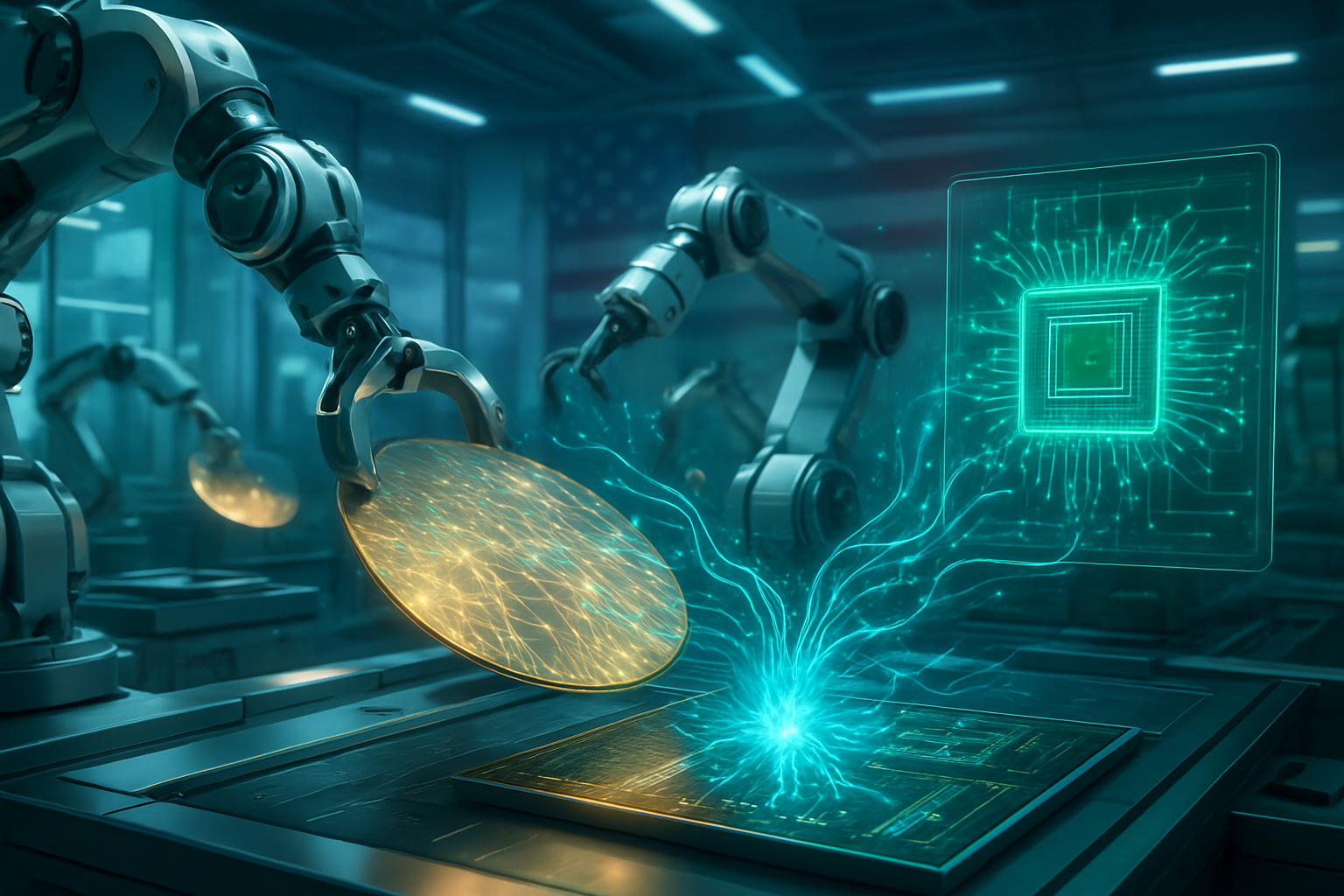
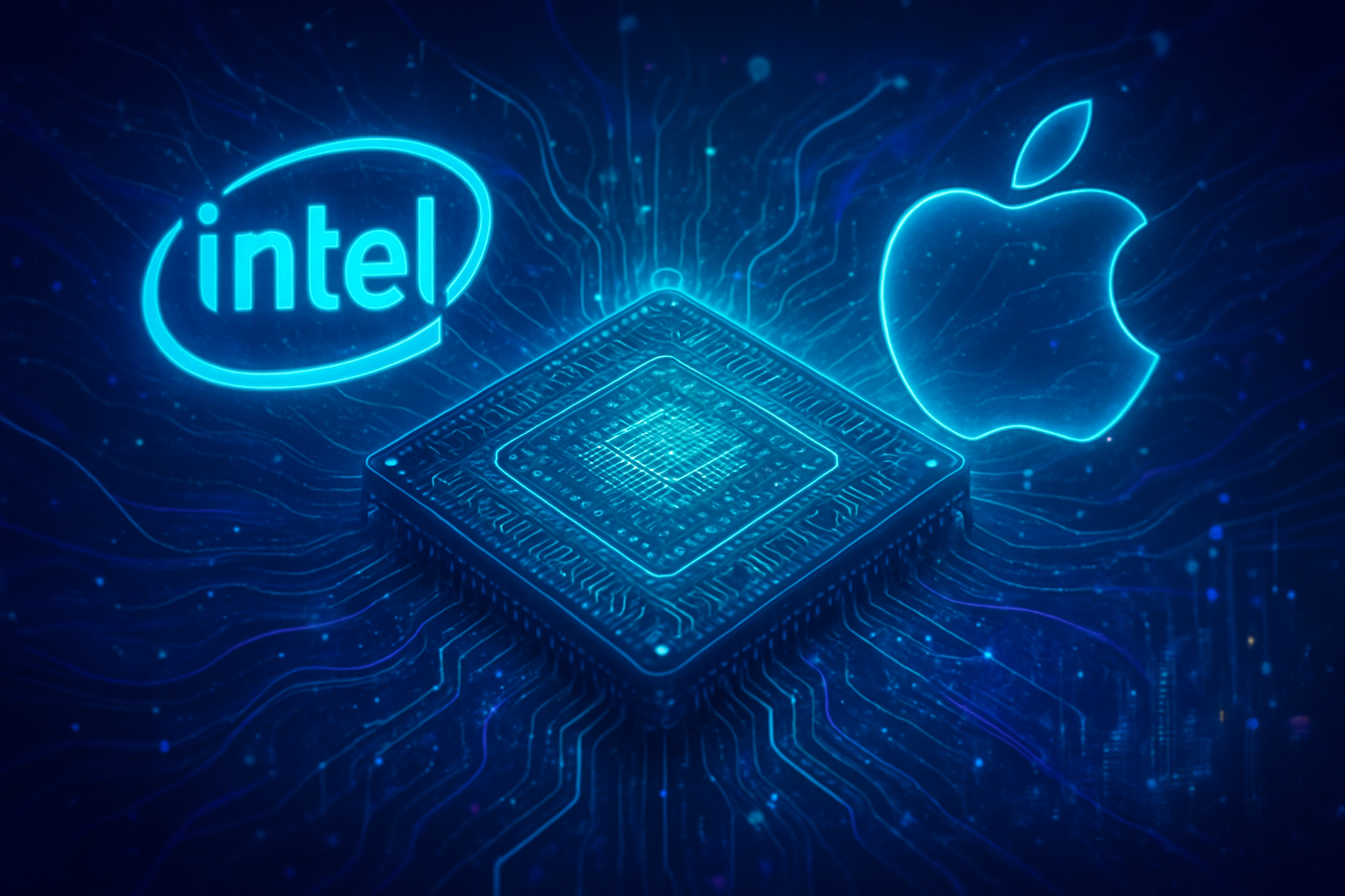
    The landscape of US chipmaking is on the cusp of a transformative shift, fueled by strategic partnerships designed to bolster domestic semiconductor production and diversify critical supply chains. At the forefront of this evolving narrative is the persistent and growing buzz around a potential landmark deal between two tech giants: Intel (NASDAQ: INTC) and Apple (NASDAQ: AAPL). This isn't a return to Apple utilizing Intel's x86 processors, but rather a strategic manufacturing alliance where Intel Foundry Services (IFS) could become a key fabricator for Apple's custom-designed M-series chips. If realized, this partnership, projected to commence as early as mid-2027, promises to reshape the domestic semiconductor industry, with profound implications for AI hardware, supply chain resilience, and global tech competition.

    This potential collaboration signifies a pivotal moment, moving beyond traditional supplier-client relationships to one of strategic interdependence in advanced manufacturing. For Apple, it represents a crucial step in de-risking its highly concentrated supply chain, currently heavily reliant on Taiwan Semiconductor Manufacturing Company (TSMC) (NYSE: TSM). For Intel, it’s a monumental validation of its aggressive foundry strategy and its ambitious roadmap to regain process leadership with cutting-edge technologies like the 18A node. The reverberations of such a deal would be felt across the entire tech ecosystem, from major AI labs to burgeoning startups, fundamentally altering market dynamics and accelerating the "Made in USA" agenda in advanced chip production.

    The Technical Backbone: Intel's 18A-P Process and Foveros Direct

    The rumored deal's technical foundation rests on Intel's cutting-edge 18A-P process node, an optimized variant of its next-generation 2nm-class technology. Intel 18A is designed to reclaim process leadership through several groundbreaking innovations. Central to this is RibbonFET, Intel's implementation of gate-all-around (GAA) transistors, which offers superior electrostatic control and scalability beyond traditional FinFET designs, promising over 15% improvement in performance per watt. Complementing this is PowerVia, a novel back-side power delivery architecture that separates power and signal routing layers, drastically reducing IR drop and enhancing signal integrity, potentially boosting transistor density by up to 30%. The "P" in 18A-P signifies performance enhancements and optimizations specifically for mobile applications, delivering an additional 8% performance per watt improvement over the base 18A node. Apple has reportedly already obtained the 18AP Process Design Kit (PDK) 0.9.1GA and is awaiting the 1.0/1.1 releases in Q1 2026, targeting initial chip shipments by Q2-Q3 2027.

    Beyond the core transistor technology, the partnership would likely leverage Foveros Direct, Intel's most advanced 3D packaging technology. Foveros Direct employs direct copper-to-copper hybrid bonding, enabling ultra-high density interconnects with a sub-10 micron pitch – a tenfold improvement over traditional methods. This allows for true vertical die stacking, integrating multiple IP chiplets, memory, and specialized compute elements in a 3D configuration. This innovation is critical for enhancing performance by reducing latency, improving bandwidth, and boosting power efficiency, all crucial for the complex, high-performance, and energy-efficient M-series chips. The 18A-P manufacturing node is specifically designed to support Foveros Direct, enabling sophisticated multi-die designs for Apple.

    This approach significantly differs from Apple's current, almost exclusive reliance on TSMC for its M-series chips. While TSMC's advanced nodes (like 5nm, 3nm, and upcoming 2nm) have powered Apple's recent successes, the Intel partnership represents a strategic diversification. Intel would initially focus on manufacturing Apple's lowest-end M-series processors (potentially M6 or M7 generations) for high-volume devices such as the MacBook Air and iPad Pro, with projected annual shipments of 15-20 million units. This allows Apple to test Intel's capabilities in less thermally constrained devices, while TSMC is expected to continue supplying the majority of Apple's higher-end, more complex M-series chips.

    Initial reactions from the semiconductor industry and analysts, particularly following reports from renowned Apple supply chain analyst Ming-Chi Kuo in late November 2025, have been overwhelmingly positive. Intel's stock saw significant jumps, reflecting increased investor confidence. The deal is widely seen as a monumental validation for Intel Foundry Services (IFS), signaling that Intel is successfully executing its aggressive roadmap to regain process leadership and attract marquee customers. While cautious optimism suggests Intel may not immediately rival TSMC's overall capacity or leadership in the absolute bleeding edge, this partnership is viewed as a crucial step in Intel's foundry turnaround and a positive long-term outlook.

    Reshaping the AI and Tech Ecosystem

    The potential Intel-Apple foundry deal would send ripples across the AI and broader tech ecosystem, altering competitive landscapes and strategic advantages. For Intel, this is a cornerstone of its turnaround strategy. Securing Apple, a prominent tier-one customer, would be a critical validation for IFS, proving its 18A process is competitive and reliable. This could attract other major chip designers like AMD (NASDAQ: AMD), NVIDIA (NASDAQ: NVDA), Qualcomm (NASDAQ: QCOM), Google (NASDAQ: GOOGL), and Amazon (NASDAQ: AMZN), accelerating IFS's path to profitability and establishing Intel as a formidable player in the foundry market against TSMC.

    Apple stands to gain significant strategic flexibility and supply chain security. Diversifying its manufacturing base reduces its vulnerability to geopolitical risks and potential production bottlenecks, ensuring a more resilient supply of its crucial M-series chips. This move also aligns with increasing political pressure for "Made in USA" components, potentially offering Apple goodwill and mitigating future regulatory challenges. While TSMC is expected to retain the bulk of high-end M-series production, Intel's involvement could introduce competition, potentially leading to better pricing and more favorable terms for Apple in the long run.

    For TSMC, while its dominance in advanced manufacturing remains strong, Intel's entry as a second-source manufacturer for Apple represents a crack in its near-monopoly. This could intensify competition, potentially putting pressure on TSMC regarding pricing and innovation, though its technological lead in certain areas may persist. The broader availability of power-efficient, M-series-like chips manufactured by Intel could also pose a competitive challenge to NVIDIA, particularly for AI inference tasks at the edge and in devices. While NVIDIA's GPUs will remain critical for large-scale cloud-based AI training, increased competition in inference could impact its market share in specific segments.

    The deal also carries implications for other PC manufacturers and tech giants increasingly developing custom silicon. The success of Intel's foundry business with Apple could encourage companies like Microsoft (NASDAQ: MSFT) (which is also utilizing Intel's 18A node for its Maia AI accelerator) to further embrace custom ARM-based AI chips, accelerating the shift towards AI-enabled PCs and mobile devices. This could disrupt the traditional CPU market by further validating ARM-based processors in client computing, intensifying competition for AMD and Qualcomm, who are also deeply invested in ARM-based designs for AI-enabled PCs.

    Wider Significance: Underpinning the AI Revolution

    This potential Intel-Apple manufacturing deal, while not an AI breakthrough in terms of design or algorithm, holds immense wider significance for the hardware infrastructure that underpins the AI revolution. The AI chip market is booming, driven by generative AI, cloud AI, and the proliferation of edge AI. Apple's M-series chips, with their integrated Neural Engines, are pivotal in enabling powerful, energy-efficient on-device AI for tasks like image generation and LLM processing. Intel, while historically lagging in AI accelerators, is aggressively pursuing a multi-faceted AI strategy, with IFS being a central pillar to enable advanced AI hardware for itself and others.

    The overall impacts are multifaceted. For Apple, it's about supply chain diversification and aligning with "Made in USA" initiatives, securing access to Intel's cutting-edge 18A process. For Intel, it's a monumental validation of its Foundry Services, boosting its reputation and attracting future tier-one customers, potentially transforming its long-term market position. For the broader AI and tech industry, it signifies increased competition in foundry services, fostering innovation and resilience in the global semiconductor supply chain. Furthermore, strengthened domestic chip manufacturing (via Intel) would be a significant geopolitical development, impacting global tech policy and trade relations, and potentially enabling a faster deployment of AI at the edge across a wide range of devices.

    However, potential concerns exist. Intel's Foundry Services has recorded significant operating losses and must demonstrate competitive yields and costs at scale with its 18A process to meet Apple's stringent demands. The deal's initial scope for Apple is reportedly limited to "lowest-end" M-series chips, meaning TSMC would likely retain the production of higher-performance variants and crucial iPhone processors. This implies Apple is diversifying rather than fully abandoning TSMC, and execution risks remain given the aggressive timeline for 18A production.

    Comparing this to previous AI milestones, this deal is not akin to the invention of deep learning or transformer architectures, nor is it a direct design innovation like NVIDIA's CUDA or Google's TPUs. Instead, its significance lies in a manufacturing and strategic supply chain breakthrough. It demonstrates the maturity and competitiveness of Intel's advanced fabrication processes, highlights the increasing influence of geopolitical factors on tech supply chains, and reinforces the trend of vertical integration in AI, where companies like Apple seek to secure the foundational hardware necessary for their AI vision. In essence, while it doesn't invent new AI, this deal profoundly impacts how cutting-edge AI-capable hardware is produced and distributed, which is an increasingly critical factor in the global race for AI dominance.

    The Road Ahead: What to Watch For

    The coming years will be crucial in observing the unfolding of this potential strategic partnership. In the near-term (2026-2027), all eyes will be on Intel's 18A process development, specifically the timely release of PDK version 1.0/1.1 in Q1 2026, which is critical for Apple's development progress. The market will closely monitor Intel's ability to achieve competitive yields and costs at scale, with initial shipments of Apple's lowest-end M-series processors expected in Q2-Q3 2027 for devices like the MacBook Air and iPad Pro.

    Long-term (beyond 2027), this deal could herald a more diversified supply chain for Apple, offering greater resilience against geopolitical shocks and reducing its sole reliance on TSMC. For Intel, successful execution with Apple could pave the way for further lucrative contracts, potentially including higher-end Apple chips or business from other tier-one customers, cementing IFS's position as a leading foundry. The "Made in USA" alignment will also be a significant long-term factor, potentially influencing government support and incentives for domestic chip production.

    Challenges remain, particularly Intel's need to demonstrate consistent profitability for its foundry division and maintain Apple's stringent standards for performance and power efficiency. Experts, notably Ming-Chi Kuo, predict that while Intel will manufacture Apple's lowest-end M-series chips, TSMC will continue to be the primary manufacturer for Apple's higher-end M-series and A-series (iPhone) chips. This is a strategic diversification for Apple and a crucial "turnaround signal" for Intel's foundry business.

    In the coming weeks and months, watch for further updates on Intel's 18A process roadmap and any official announcements from either Intel or Apple regarding this partnership. Observe the performance and adoption of new Windows on ARM devices, as their success will indicate the broader shift in the PC market. Finally, keep an eye on new and more sophisticated AI applications emerging across macOS and iOS that fully leverage the on-device processing power of Apple's Neural Engine, showcasing the practical benefits of powerful edge AI and the hardware that enables it.


    This content is intended for informational purposes only and represents analysis of current AI developments.

    TokenRing AI delivers enterprise-grade solutions for multi-agent AI workflow orchestration, AI-powered development tools, and seamless remote collaboration platforms.
    For more information, visit https://www.tokenring.ai/.

  • Smartkem and Jericho Energy Ventures Forge U.S.-Owned AI Infrastructure Powerhouse in Proposed Merger

    Smartkem and Jericho Energy Ventures Forge U.S.-Owned AI Infrastructure Powerhouse in Proposed Merger

    San Jose, CA – November 20, 2025 – In a strategic move poised to reshape the landscape of artificial intelligence infrastructure, Smartkem (NASDAQ: SMTK) and Jericho Energy Ventures (TSX-V: JEV, OTC: JROOF) have announced a proposed all-stock merger. The ambitious goal: to create a U.S.-owned and controlled AI-focused infrastructure company, leveraging cutting-edge semiconductor innovations for the next generation of AI data centers. This merger, initially outlined in a non-binding Letter of Intent (LOI) signed on October 7, 2025, and extended on November 20, 2025, aims to address the escalating demand for AI compute capacity by vertically integrating energy supply with advanced semiconductor materials and packaging.

    The combined entity seeks to deliver faster, more efficient, and resilient AI infrastructure by marrying Smartkem's patented organic semiconductor technology with Jericho's scalable energy platform. This synergistic approach is designed to tackle the formidable challenges of power consumption, heat management, and cost associated with the exponential growth of AI, promising a new era of sustainable and high-performance AI computing within a secure, domestic framework.

    Technical Synergy: Powering AI with Organic Semiconductors and Resilient Energy

    The heart of this proposed merger lies in the profound technical synergy between Smartkem's advanced materials and Jericho Energy Ventures' robust energy solutions. Smartkem's contribution is centered on its proprietary TRUFLEX® semiconductor polymers, a groundbreaking class of organic thin-film transistors (OTFTs). Unlike traditional inorganic semiconductors that demand high processing temperatures (often exceeding 300°C), TRUFLEX materials enable ultra-low temperature printing processes (as low as 80°C). These liquid polymers can be solution-deposited onto cost-effective plastic or glass substrates, allowing for panel-level packaging that can accommodate hundreds of AI chips on larger panels, a significant departure from the limited yields of 300mm silicon wafers. This innovation is expected to drastically reduce manufacturing costs and energy consumption for semiconductor components, while also improving throughput and cost efficiency per chip.

    Smartkem's technology is poised to revolutionize several critical aspects of AI infrastructure:

    • Advanced AI Chip Packaging: By reducing power consumption and heat at the chip level, Smartkem's organic semiconductors are vital for creating denser, more powerful AI accelerators.
    • Low-Power Optical Data Transmission: The technology facilitates faster and more energy-efficient interconnects within data centers, crucial for the rapid communication required by large AI models.
    • Conformable Sensors: The versatility extends to developing flexible sensors for environmental monitoring and ensuring operational resilience within data centers.

    Jericho Energy Ventures complements this with its expertise in providing scalable, resilient, and low-cost energy. JEV leverages its extensive portfolio of long-producing oil and gas joint venture assets and infrastructure in Oklahoma. By harnessing abundant, low-cost on-site natural gas for behind-the-meter power, JEV aims to transform these assets into secure, high-performance AI computing hubs. Their build-to-suit data centers are strategically located on a U.S. fiber "superhighway," ensuring high-speed connectivity. Furthermore, JEV is actively investing in clean energy, including hydrogen technologies, with subsidiaries like Hydrogen Technologies developing zero-emission boiler technology and Etna Solutions working on green hydrogen production, signaling a future pathway for more sustainable energy integration.

    This integrated approach differentiates itself from previous fragmented systems by offering a unified, vertically integrated platform that addresses both the hardware and power demands of AI. This holistic design, from energy supply to advanced semiconductor materials, aims to deliver significantly more energy-efficient, scalable, and cost-effective AI computing power than conventional methods.

    Reshaping the AI Competitive Landscape

    The proposed merger between Smartkem and Jericho Energy Ventures carries significant implications for AI companies, tech giants, and startups alike, potentially introducing a new paradigm in the AI infrastructure market.

    The creation of a vertically integrated, U.S.-owned entity for AI data centers could intensify competition for established players in the semiconductor and cloud computing sectors. Tech giants like Nvidia (NASDAQ: NVDA), Intel (NASDAQ: INTC), AMD (NASDAQ: AMD) in semiconductors, and cloud providers such as Amazon (NASDAQ: AMZN) (AWS), Google (NASDAQ: GOOGL) (GCP), and Microsoft (NASDAQ: MSFT) (Azure) could face a new, formidable alternative. The merged company's focus on energy-efficient AI chip packaging and resilient, low-cost power solutions could offer a compelling alternative, potentially leading to supply chain diversification for major players seeking to reduce reliance on a limited number of providers. This could also spur partnerships or even future acquisitions if the technology proves disruptive and scalable.

    For AI startups, this development could be a double-edged sword. On one hand, if the combined entity successfully delivers more energy-efficient and cost-effective AI infrastructure, it could lower the operational costs associated with advanced AI development, making high-end AI compute more accessible. This could foster innovation by allowing startups to allocate more resources to model development and applications rather than grappling with prohibitive infrastructure expenses. On the other hand, a powerful, vertically integrated player could also intensify competition for talent, funding, and market share, especially for startups operating in niche areas of AI chip packaging or energy solutions for data centers.

    Companies that stand to benefit most include AI data center operators seeking improved efficiency and resilience, and AI hardware developers looking for advanced, cost-effective chip packaging solutions. Crucially, as a U.S.-owned and controlled entity, the combined company is strategically positioned to benefit from government initiatives and incentives aimed at bolstering domestic AI infrastructure and securing critical supply chains. This market positioning offers a unique competitive advantage, appealing to clients and government contracts prioritizing domestic sourcing and secure infrastructure for their AI initiatives.

    A Broader Stroke on the AI Canvas

    The Smartkem Jericho merger is more than just a corporate transaction; it represents a significant development within the broader AI landscape, addressing some of the most pressing challenges facing the industry. Its emphasis on energy efficiency and a U.S.-owned infrastructure aligns perfectly with the growing global trend towards "Green AI" and responsible technological development. As AI models continue to grow in complexity and scale, their energy footprint has become a major concern. By offering an inherently more energy-efficient infrastructure, this initiative could pave the way for more sustainable AI development and deployment.

    The strategic importance of a U.S.-owned AI infrastructure cannot be overstated. In an era of increasing geopolitical competition, ensuring domestic control over foundational AI technologies is crucial for national security, economic competitiveness, and technological leadership. Jericho's leveraging of domestic energy assets, including a future pathway to clean hydrogen, contributes significantly to energy independence for critical AI operations. This helps mitigate risks associated with foreign supply chain dependencies and ensures a resilient, low-cost power supply for the surging demand from AI compute growth within the U.S. The U.S. government is actively seeking to expand AI-ready data centers domestically, and this merger fits squarely within that national strategy.

    While the potential is immense, the merger faces significant hurdles. The current non-binding Letter of Intent means the deal is not yet finalized and requires substantial additional capital, rigorous due diligence, and approvals from boards, stockholders, and regulatory bodies. Smartkem's publicly reported financial challenges, including substantial losses and a high-risk financial profile, underscore the need for robust funding and a seamless integration strategy. The scalability of organic semiconductor manufacturing to meet the immense global demand for AI, and the complexities of integrating a novel energy platform with existing data center standards are also considerable operational challenges.

    If successful, this merger could be compared to previous AI infrastructure milestones, such as the advent of GPUs for parallel processing or the development of specialized AI accelerators (ASICs). It aims to introduce a fundamentally new material and architectural approach to how AI hardware is built and powered, potentially leading to significant gains in performance per watt and overall efficiency, marking a similar strategic shift in the evolution of AI.

    The Road Ahead: Anticipated Developments and Challenges

    The proposed Smartkem and Jericho Energy Ventures merger sets the stage for a series of transformative developments in the AI infrastructure domain, both in the near and long term. In the immediate future, the combined entity will likely prioritize the engineering and deployment of energy-efficient AI data centers specifically designed for demanding next-generation workloads. This will involve the rapid integration of Smartkem's advanced AI chip packaging solutions, aimed at reducing power consumption and heat, alongside the implementation of low-power optical data transmission for faster internal data center interconnects. The initial focus will also be on establishing conformable sensors for enhanced environmental monitoring and operational resilience within these new facilities, solidifying the vertically integrated platform from energy supply to semiconductor materials.

    Looking further ahead, the long-term vision is to achieve commercial scale for Smartkem's organic semiconductors within AI computing, fully realizing the potential of its patented platform. This will be crucial for delivering on the promise of foundational infrastructure necessary for scalable AI, with the ultimate goal of offering faster, cleaner, and more resilient AI facilities. This aligns with the broader industry push towards "Green AI," aiming to make advanced AI more accessible and sustainable by accelerating previously compute-bound applications. Potential applications extend beyond core data centers to specialized AI hardware, advanced manufacturing, and distributed AI systems requiring efficient, low-power processing.

    However, the path forward is fraught with challenges. The most immediate hurdle is the finalization of the merger itself, which remains contingent on a definitive agreement, successful due diligence, significant additional capital, and various corporate and regulatory approvals. Smartkem's publicly reported financial health, including substantial losses and a high-risk financial profile, highlights the critical need for robust funding and a seamless integration plan. Operational challenges include scaling organic semiconductor manufacturing to meet the immense global demand for AI, navigating complex energy infrastructure regulations, and ensuring the seamless integration of Jericho's energy platform with evolving data center standards. Furthermore, Smartkem's pivot from display materials to AI packaging and optical links requires new proof points and rigorous qualification processes, which are typically long-cycle in the semiconductor industry.

    Experts predict that specialized, vertically integrated infrastructure solutions, such as those proposed by Smartkem and Jericho, will become increasingly vital to sustain the rapid pace of AI innovation. The emphasis on sustainability and cost-effectiveness in future AI infrastructure is paramount, and this merger reflects a growing trend of cross-sector collaborations aimed at capitalizing on the burgeoning AI market. Observers anticipate more such partnerships as the industry adapts to shifting demands and seeks to carve out shares of the global AI infrastructure market. The market has shown initial optimism, with Smartkem's shares rising post-announcement, indicating investor confidence in the potential for growth, though the successful execution and financial stability remain critical factors to watch closely.

    A New Horizon for AI Infrastructure

    The proposed all-stock merger between Smartkem (NASDAQ: SMTK) and Jericho Energy Ventures (TSX-V: JEV, OTC: JROOF) marks a potentially pivotal moment in the evolution of AI infrastructure. By aiming to create a U.S.-owned, AI-focused entity that vertically integrates advanced organic semiconductor technology with scalable, resilient energy solutions, the combined company is positioning itself to address the fundamental challenges of power, efficiency, and cost in the age of exponential AI growth.

    The significance of this development in AI history could be profound. If successful, it represents a departure from incremental improvements in traditional silicon-based infrastructure, offering a new architectural paradigm that promises to deliver faster, cleaner, and more resilient AI compute capabilities. This could not only democratize access to high-end AI for a broader range of innovators but also fortify the U.S.'s strategic position in the global AI race through enhanced national security and energy independence.

    In the coming weeks and months, all eyes will be on the progress of the definitive merger agreement, the securing of necessary capital, and the initial steps towards integrating these two distinct yet complementary technologies. The ability of the merged entity to overcome financial and operational hurdles, scale its innovative organic semiconductor manufacturing, and seamlessly integrate its energy solutions will determine its long-term impact. This merger signifies a bold bet on a future where AI's insatiable demand for compute power is met with equally innovative and sustainable infrastructure solutions.


    This content is intended for informational purposes only and represents analysis of current AI developments.

    TokenRing AI delivers enterprise-grade solutions for multi-agent AI workflow orchestration, AI-powered development tools, and seamless remote collaboration platforms.
    For more information, visit https://www.tokenring.ai/.

  • TSMC’s Arizona Bet: Forging America’s AI Chip Future with Unprecedented Investment

    TSMC’s Arizona Bet: Forging America’s AI Chip Future with Unprecedented Investment

    Phoenix, AZ – November 3, 2025 – Taiwan Semiconductor Manufacturing Company (TSMC) (NYSE: TSM) is dramatically reshaping the landscape of advanced semiconductor manufacturing in the United States, cementing its pivotal role in bolstering American capabilities, particularly in the burgeoning field of artificial intelligence. With an unprecedented commitment now reaching US$165 billion, TSMC's expanded investment in Arizona signifies a monumental strategic shift, aiming to establish a robust, end-to-end domestic supply chain for cutting-edge AI chips. This move is not merely an expansion; it's a foundational build-out designed to secure U.S. leadership in AI, enhance national security through supply chain resilience, and create tens of thousands of high-tech jobs.

    This aggressive push by the world's leading contract chipmaker comes at a critical juncture, as global demand for advanced AI accelerators continues to skyrocket. The immediate significance of TSMC's U.S. endeavor is multi-faceted: it promises to bring the most advanced chip manufacturing processes, including 3-nanometer (N3) and 2-nanometer (N2) technologies, directly to American soil. This onshoring effort, heavily supported by the U.S. government's CHIPS and Science Act, aims to reduce geopolitical risks, shorten lead times for critical components, and foster a vibrant domestic ecosystem capable of supporting the next generation of AI innovation. The recent celebration of the first NVIDIA (NASDAQ: NVDA) Blackwell wafer produced on U.S. soil at TSMC's Phoenix facility in October 2025 underscored this milestone, signaling a new era of domestic advanced AI chip production.

    A New Era of Domestic Advanced Chipmaking: Technical Prowess Takes Root in Arizona

    TSMC's expanded Arizona complex is rapidly evolving into a cornerstone of U.S. advanced semiconductor manufacturing, poised to deliver unparalleled technical capabilities crucial for the AI revolution. The initial investment has blossomed into a three-fab strategy, complemented by plans for advanced packaging facilities and a significant research and development center, all designed to create a comprehensive domestic AI supply chain. This represents a stark departure from previous reliance on overseas fabrication, bringing the most sophisticated processes directly to American shores.

    The first fab at TSMC Arizona commenced high-volume production of 4-nanometer (N4) process technology in late 2024, a significant step that immediately elevated the U.S.'s domestic advanced chipmaking capacity. Building on this, the structure for the second fab was completed in 2025 and is targeted to begin volume production of 3-nanometer (N3) technology in 2028, with plans to produce the world's most advanced 2-nanometer (N2) process technology. Furthermore, TSMC broke ground on a third fab in April 2025, which is projected to produce chips using 2nm or even more advanced processes, such as A16, with production expected to begin by the end of the decade. Each of these advanced fabs is designed with cleanroom areas approximately double the size of an industry-standard logic fab, reflecting the scale and complexity of modern chip manufacturing.

    This domestic manufacturing capability is a game-changer for AI chip design. Companies like NVIDIA (NASDAQ: NVDA), a key TSMC partner, rely heavily on these leading-edge process technologies to pack billions of transistors onto their graphics processing units (GPUs) and AI accelerators. The N3 and N2 nodes offer significant improvements in transistor density, power efficiency, and performance over previous generations, directly translating to more powerful and efficient AI models. This differs from previous approaches where such advanced fabrication was almost exclusively concentrated in Taiwan, introducing potential logistical and geopolitical vulnerabilities. The onshoring of these capabilities means closer collaboration between U.S.-based chip designers and manufacturers, potentially accelerating innovation cycles and streamlining supply chains.

    Initial reactions from the AI research community and industry experts have been overwhelmingly positive, albeit with a pragmatic understanding of the challenges involved. The ability to source cutting-edge AI chips domestically is seen as a critical enabler for national AI strategies and a safeguard against supply chain disruptions. Experts highlight that while the upfront costs and complexities of establishing such facilities are immense, the long-term strategic advantages in terms of innovation, security, and economic growth far outweigh them. The U.S. government's substantial financial incentives through the CHIPS Act, including up to US$6.6 billion in direct funding and US$5 billion in loans, underscore the national importance of this endeavor.

    Reshaping the AI Industry Landscape: Beneficiaries and Competitive Shifts

    TSMC's burgeoning U.S. advanced manufacturing footprint is poised to profoundly impact the competitive dynamics within the artificial intelligence industry, creating clear beneficiaries and potentially disrupting existing market positions. The direct availability of cutting-edge fabrication on American soil will provide strategic advantages to companies heavily invested in AI hardware, while also influencing the broader tech ecosystem.

    Foremost among the beneficiaries are U.S.-based AI chip design powerhouses such as NVIDIA (NASDAQ: NVDA), Advanced Micro Devices (NASDAQ: AMD), Apple (NASDAQ: AAPL), Broadcom (NASDAQ: AVGO), and Qualcomm (NASDAQ: QCOM). These companies are TSMC's largest customers and rely on its advanced process technologies to bring their innovative AI accelerators, CPUs, and specialized chips to market. Having a domestic source for their most critical components reduces logistical complexities, shortens supply chains, and mitigates risks associated with geopolitical tensions, particularly concerning the Taiwan Strait. For NVIDIA, whose Blackwell platform chips are now being produced on U.S. soil at TSMC Arizona, this means a more resilient and potentially faster pathway to deliver the hardware powering the next generation of AI.

    The competitive implications for major AI labs and tech companies are significant. Access to advanced, domestically produced chips can accelerate the development and deployment of new AI models and applications. Companies that can quickly iterate and scale their hardware will gain a competitive edge in the race for AI dominance. This could also indirectly benefit cloud service providers like Amazon (NASDAQ: AMZN) AWS, Microsoft (NASDAQ: MSFT) Azure, and Google (NASDAQ: GOOGL) Cloud, who are heavily investing in AI infrastructure and custom silicon, by providing them with a more secure and diversified supply of high-performance chips.

    Potential disruption to existing products or services could arise from increased competition and faster innovation cycles. As more advanced chips become readily available, companies might be able to offer more powerful AI-driven features, potentially rendering older hardware or less optimized services less competitive. Furthermore, this move could bolster the efforts of Intel (NASDAQ: INTC) Foundry Services, which is also aggressively pursuing advanced manufacturing in the U.S. While TSMC and Intel are competitors in the foundry space, TSMC's presence helps to build out the overall U.S. supply chain ecosystem, from materials to equipment, which could indirectly benefit all domestic manufacturers.

    In terms of market positioning and strategic advantages, TSMC's U.S. expansion solidifies its role as an indispensable partner for American tech giants. It allows these companies to claim "Made in USA" for critical AI components, a powerful marketing and strategic advantage in an era focused on national industrial capabilities. This strategic alignment between TSMC and its U.S. customers strengthens the entire American technology sector, positioning it for sustained leadership in the global AI race.

    Wider Significance: Anchoring America's AI Future and Global Semiconductor Rebalancing

    TSMC's ambitious expansion in the United States transcends mere manufacturing; it represents a profound rebalancing act within the global semiconductor landscape and a critical anchor for America's long-term AI strategy. This initiative fits squarely into the broader trend of nations seeking to secure their technology supply chains and foster domestic innovation, particularly in strategic sectors like AI.

    The impacts of this development are far-reaching. Geopolitically, it significantly de-risks the global technology supply chain by diversifying advanced chip production away from a single region. The concentration of cutting-edge fabrication in Taiwan has long been a point of vulnerability, and TSMC's U.S. fabs offer a crucial layer of resilience against potential disruptions, whether from natural disasters or geopolitical tensions. This move directly supports the U.S. government's push for "chip sovereignty," a national security imperative aimed at ensuring access to the most advanced semiconductors for defense, economic competitiveness, and AI leadership.

    Economically, the investment is a massive boon, projected to generate approximately 40,000 construction jobs over the next four years and tens of thousands of high-paying, high-tech jobs in advanced chip manufacturing and R&D. It is also expected to drive more than $200 billion of indirect economic output in Arizona and across the United States within the next decade. This fosters a robust ecosystem, attracting ancillary industries and talent, and revitalizing American manufacturing prowess in a critical sector.

    Potential concerns, however, do exist. The cost of manufacturing in the U.S. is significantly higher than in Taiwan, leading to initial losses for TSMC's Arizona facility. This highlights challenges related to labor costs, regulatory environments, and the maturity of the local supply chain for specialized materials and equipment. While the CHIPS Act provides substantial subsidies, the long-term economic viability without continuous government support remains a subject of debate for some analysts. Furthermore, while advanced wafers are being produced, the historical necessity of sending them back to Taiwan for advanced packaging has been a bottleneck in achieving a truly sovereign supply chain. However, TSMC's plans for U.S. advanced packaging facilities and partnerships with companies like Amkor aim to address this gap.

    Compared to previous AI milestones and breakthroughs, TSMC's U.S. expansion provides the foundational hardware infrastructure that underpins all software-level advancements. While breakthroughs in AI algorithms or models often grab headlines, the ability to physically produce the processors that run these models is equally, if not more, critical. This initiative is comparable in strategic importance to the establishment of Silicon Valley itself, creating the physical infrastructure for the next wave of technological innovation. It signals a shift from purely design-centric innovation in the U.S. to a more integrated design-and-manufacturing approach for advanced technologies.

    The Road Ahead: Future Developments and AI's Hardware Horizon

    The establishment of TSMC's advanced manufacturing complex in Arizona sets the stage for a dynamic period of future developments, promising to further solidify the U.S.'s position at the forefront of AI innovation. The near-term and long-term outlook involves not only the ramp-up of current facilities but also the potential for even more advanced technologies and a fully integrated domestic supply chain.

    In the near term, the focus will be on the successful ramp-up of the first fab's 4nm production and the continued construction and equipping of the second and third fabs. The second fab is slated to begin volume production of 3nm technology in 2028, with the subsequent introduction of 2nm process technology. The third fab, broken ground in April 2025, aims for production of 2nm or A16 processes by the end of the decade. This aggressive timeline indicates a commitment to bringing the absolute leading edge of semiconductor technology to the U.S. rapidly. Furthermore, the development of the planned two advanced packaging facilities is critical; these will enable the complete "chiplet" integration and final assembly of complex AI processors domestically, addressing the current challenge of needing to send wafers back to Taiwan for packaging.

    Potential applications and use cases on the horizon are vast. With a reliable domestic source of 2nm and A16 chips, American companies will be able to design and deploy AI systems with unprecedented computational power and energy efficiency. This will accelerate breakthroughs in areas such as generative AI, autonomous systems, advanced robotics, personalized medicine, and scientific computing. The ability to quickly prototype and manufacture specialized AI hardware could also foster a new wave of startups focused on niche AI applications requiring custom silicon.

    However, significant challenges need to be addressed. Workforce development remains paramount; training a skilled labor force capable of operating and maintaining these highly complex fabs is a continuous effort. TSMC is actively engaged in partnerships with local universities and community colleges to build this talent pipeline. High operating costs in the U.S. compared to Asia will also require ongoing innovation in efficiency and potentially continued government support to maintain competitiveness. Furthermore, the development of a complete domestic supply chain for all materials, chemicals, and equipment needed for advanced chip manufacturing will be a long-term endeavor, requiring sustained investment across the entire ecosystem.

    Experts predict that the success of TSMC's Arizona venture will serve as a blueprint for future foreign direct investment in strategic U.S. industries. It is also expected to catalyze further domestic investment from related industries, creating a virtuous cycle of growth and innovation. The long-term vision is a self-sufficient U.S. semiconductor ecosystem that can design, manufacture, and package the world's most advanced chips, ensuring national security and economic prosperity.

    A New Dawn for American Semiconductor Independence

    TSMC's monumental investment in U.S. advanced AI chip manufacturing marks a pivotal moment in the history of American technology and global semiconductor dynamics. The commitment, now totaling an astounding US$165 billion across three fabs, advanced packaging facilities, and an R&D center in Arizona, is a strategic imperative designed to forge a resilient, sovereign supply chain for the most critical components of the AI era. This endeavor, strongly supported by the U.S. government through the CHIPS and Science Act, underscores a national recognition of the strategic importance of advanced chip fabrication.

    The key takeaways are clear: the U.S. is rapidly building its capacity for cutting-edge chip production, moving from a heavy reliance on overseas manufacturing to a more integrated domestic approach. This includes bringing 4nm, 3nm, and eventually 2nm and A16 process technologies to American soil, directly benefiting leading U.S. AI companies like NVIDIA (NASDAQ: NVDA), AMD (NASDAQ: AMD), and Apple (NASDAQ: AAPL). The economic impact is projected to be transformative, creating tens of thousands of high-paying jobs and driving hundreds of billions in economic output. Geopolitically, it significantly de-risks the global supply chain and bolsters U.S. national security.

    This development's significance in AI history cannot be overstated. It provides the essential hardware foundation for the next generation of artificial intelligence, enabling more powerful, efficient, and secure AI systems. It represents a tangible step towards American technological independence and a reassertion of its manufacturing prowess in the most advanced sectors. While challenges such as workforce development and high operating costs persist, the strategic benefits of this investment are paramount.

    In the coming weeks and months, the focus will remain on the continued progress of construction, the successful ramp-up of production at the first fab, and the ongoing development of the necessary talent pipeline. What to watch for includes further announcements regarding advanced packaging capabilities, potential new partnerships within the U.S. ecosystem, and how quickly these domestic fabs can achieve cost-efficiency and scale comparable to their Taiwanese counterparts. TSMC's Arizona bet is not just about making chips; it's about building the future of American innovation and securing its leadership in the AI-powered world.


    This content is intended for informational purposes only and represents analysis of current AI developments.

    TokenRing AI delivers enterprise-grade solutions for multi-agent AI workflow orchestration, AI-powered development tools, and seamless remote collaboration platforms.
    For more information, visit https://www.tokenring.ai/.

  • Silicon Dreams, American Hurdles: The Monumental Challenge of Building New Chip Fabs in the U.S.

    Silicon Dreams, American Hurdles: The Monumental Challenge of Building New Chip Fabs in the U.S.

    The ambition to revitalize domestic semiconductor manufacturing in the United States faces an arduous journey, particularly for new entrants like Substrate. While government initiatives aim to re-shore chip production, the path to establishing state-of-the-art fabrication facilities (fabs) is fraught with a formidable array of financial, operational, and human capital obstacles. These immediate and significant challenges threaten to derail even the most innovative ventures, highlighting the deep-seated complexities of the global semiconductor ecosystem and the immense difficulty of competing with established, decades-old supply chains.

    The vision of new companies bringing cutting-edge chip production to American soil is a potent one, promising economic growth, national security, and technological independence. However, the reality involves navigating colossal capital requirements, protracted construction timelines, a critical shortage of skilled labor, and intricate global supply chain dependencies. For a startup, these hurdles are amplified, demanding not just groundbreaking technology but also unprecedented resilience and access to vast resources to overcome the inherent inertia of an industry built on decades of specialized expertise and infrastructure concentrated overseas.

    The Technical Gauntlet: Unpacking Fab Establishment Complexities

    Establishing a modern semiconductor fab is a feat of engineering and logistical mastery, pushing the boundaries of precision manufacturing. For new companies, the technical challenges are multifaceted, starting with the sheer scale of investment required. A single, state-of-the-art fab can demand an investment upwards of $10 billion to $20 billion, encompassing not only vast cleanroom facilities but also highly specialized equipment. For instance, advanced lithography machines, critical for etching circuit patterns onto silicon wafers, can cost up to $130 million each. New players must contend with these astronomical costs, which are typically borne by established giants with deep pockets and existing revenue streams.

    The technical specifications for a new fab are incredibly stringent. Cleanrooms must maintain ISO Class 1 or lower standards, meaning fewer than 10 particles of 0.1 micrometers or larger per cubic meter of air – an environment thousands of times cleaner than a surgical operating room. Achieving and maintaining this level of purity requires sophisticated air filtration systems, specialized materials, and rigorous protocols. Moreover, the manufacturing process itself involves thousands of precise steps, from chemical vapor deposition and etching to ion implantation and metallization, each requiring absolute control over temperature, pressure, and chemical composition. Yield management, the process of maximizing the percentage of functional chips from each wafer, is an ongoing technical battle that can take years to optimize, directly impacting profitability.

    New companies like Substrate, reportedly exploring novel approaches such as particle acceleration for lithography, face an even steeper climb. While such innovations could theoretically disrupt the dominance of existing technologies (like ASML (AMS:ASML) Holding N.V.'s extreme ultraviolet (EUV) lithography), they introduce an entirely new set of technical risks and validation requirements. Unlike established players who incrementally refine proven processes, a new entrant with a revolutionary technology must not only build a fab but also simultaneously industrialize an unproven manufacturing paradigm. This requires developing an entirely new ecosystem of compatible materials, equipment, and expertise, a stark contrast to the existing, mature supply chains that support conventional chipmaking. Initial reactions from the broader AI research and semiconductor community to such radical departures are often a mix of cautious optimism and skepticism, given the immense capital and time historically required to bring any new fab technology to fruition.

    Competitive Pressures and Market Realities for Innovators

    The establishment of new semiconductor fabs in the U.S. carries significant implications for a wide array of companies, from burgeoning startups to entrenched tech giants. For new companies like Substrate, the ability to successfully navigate the immense hurdles of fab construction and operation could position them as critical players in a re-shored domestic supply chain. However, the competitive landscape is dominated by titans such as Intel (NASDAQ:INTC), Taiwan Semiconductor Manufacturing Company (TSMC) (NYSE:TSM), and Samsung (KRX:005930), all of whom are also investing heavily in U.S. fabrication capabilities, often with substantial government incentives. These established players benefit from decades of experience, existing intellectual property, vast financial resources, and deeply integrated global supply chains, making direct competition incredibly challenging for a newcomer.

    The competitive implications for major AI labs and tech companies are profound. A robust domestic chip manufacturing base could reduce reliance on overseas production, mitigating geopolitical risks and supply chain vulnerabilities that have plagued industries in recent years. Companies reliant on advanced semiconductors, from NVIDIA (NASDAQ:NVDA) and Advanced Micro Devices (NASDAQ:AMD) to Apple (NASDAQ:AAPL) and Google (NASDAQ:GOOGL), stand to benefit from more resilient and potentially faster access to cutting-edge chips. However, for new fab entrants, the challenge lies in attracting these major customers who typically prefer the reliability, proven yields, and cost-effectiveness offered by established foundries. Disrupting existing product or service supply chains requires not just a viable alternative, but one that offers a compelling advantage in performance, cost, or specialization.

    Market positioning for a new fab company in the U.S. necessitates a clear strategic advantage. This could involve specializing in niche technologies, high-security chips for defense, or developing processes that are uniquely suited for emerging AI hardware. However, without the scale of a TSMC or Intel, achieving cost parity is nearly impossible, as the semiconductor industry thrives on economies of scale. Strategic advantages might therefore hinge on superior performance for specific applications, faster turnaround times for prototyping, or a completely novel manufacturing approach that significantly reduces power consumption or increases chip density. The potential disruption to existing services would come if a new entrant could offer a truly differentiated product or a more secure supply chain, but the path to achieving such differentiation while simultaneously building a multi-billion-dollar facility is exceptionally arduous.

    The Broader AI Landscape and Geopolitical Imperatives

    The drive to establish new semiconductor factories in the United States, particularly by novel players, fits squarely within the broader AI landscape and ongoing geopolitical shifts. The insatiable demand for advanced AI chips, essential for everything from large language models to autonomous systems, has underscored the strategic importance of semiconductor manufacturing. The concentration of leading-edge fab capacity in East Asia has become a significant concern for Western nations, prompting initiatives like the U.S. CHIPS and Science Act. This act aims to incentivize domestic production, viewing it not just as an economic endeavor but as a matter of national security and technological sovereignty. The success or failure of new companies like Substrate in this environment will be a bellwether for the effectiveness of such policies.

    The impacts of successful new fab establishments would be far-reaching. A more diversified and resilient global semiconductor supply chain could alleviate future chip shortages, stabilize pricing, and foster greater innovation by providing more options for chip design companies. For the AI industry, this could translate into faster access to specialized AI accelerators, potentially accelerating research and development cycles. However, potential concerns abound. The sheer cost and complexity mean that even with government incentives, the total cost of ownership for U.S.-based fabs remains significantly higher than in regions like Taiwan. This could lead to higher chip prices, potentially impacting the affordability of AI hardware and the competitiveness of U.S.-based AI companies in the global market. There are also environmental concerns, given the immense water and energy demands of semiconductor manufacturing, which could strain local resources.

    Comparing this drive to previous AI milestones, the current push for domestic chip production is less about a single technological breakthrough and more about establishing the foundational infrastructure necessary for future AI advancements. While previous milestones focused on algorithmic improvements (e.g., deep learning, transformer architectures), this effort addresses the physical limitations of scaling AI. The ambition to develop entirely new manufacturing paradigms (like Substrate's potential particle acceleration lithography) echoes the disruptive potential seen in earlier AI breakthroughs, where novel approaches fundamentally changed what was possible. However, unlike software-based AI advancements that can scale rapidly with minimal capital, hardware innovation in semiconductors requires monumental investment and decades of refinement, making the path to widespread adoption much slower and more capital-intensive.

    Future Horizons: What Lies Ahead for Domestic Chip Production

    The coming years are expected to bring a dynamic interplay of government incentives, technological innovation, and market consolidation within the U.S. semiconductor manufacturing landscape. In the near term, we will likely see the ramp-up of existing projects by major players like Intel (NASDAQ:INTC) and TSMC (NYSE:TSM) in Arizona and Ohio, benefiting from CHIPS Act funding. For new companies like Substrate, the immediate future will involve securing substantial additional funding, navigating stringent regulatory processes, and attracting a highly specialized workforce. Experts predict a continued focus on workforce development programs and collaborations between industry and academia to address the critical talent shortage. Long-term developments could include the emergence of highly specialized fabs catering to specific AI hardware needs, or the successful commercialization of entirely new manufacturing technologies that promise greater efficiency or lower costs.

    Potential applications and use cases on the horizon for U.S.-made chips are vast. Beyond general-purpose CPUs and GPUs, there's a growing demand for custom AI accelerators, neuromorphic chips, and secure chips for defense and critical infrastructure. A robust domestic manufacturing base could enable rapid prototyping and iteration for these specialized components, giving U.S. companies a strategic edge in developing next-generation AI systems. Furthermore, advanced packaging technologies, which integrate multiple chiplets into a single, powerful package, are another area ripe for domestic investment and innovation, potentially reducing reliance on overseas back-end processes.

    However, significant challenges remain. The cost differential between U.S. and Asian manufacturing facilities is a persistent hurdle that needs to be addressed through sustained government support and technological advancements that improve efficiency. The environmental impact of large-scale fab operations, particularly concerning water consumption and energy use, will require innovative solutions in sustainable manufacturing. Experts predict that while the U.S. will likely increase its share of global semiconductor production, it is unlikely to fully decouple from the global supply chain, especially for specialized materials and equipment. The focus will remain on creating a more resilient, rather than entirely independent, ecosystem. What to watch for next includes the successful operationalization of new fabs, the effectiveness of workforce training initiatives, and any significant breakthroughs in novel manufacturing processes that could genuinely level the playing field for new entrants.

    A New Era for American Silicon: A Comprehensive Wrap-Up

    The endeavor to establish new semiconductor factories in the United States, particularly by innovative startups like Substrate, represents a pivotal moment in the nation's technological and economic trajectory. The key takeaways underscore the immense scale of the challenge: multi-billion-dollar investments, years-long construction timelines, a severe shortage of skilled labor, and the intricate web of global supply chains. Despite these formidable obstacles, the strategic imperative driven by national security and the burgeoning demands of artificial intelligence continues to fuel this ambitious re-shoring effort. The success of these ventures will not only reshape the domestic manufacturing landscape but also profoundly influence the future trajectory of AI development.

    This development's significance in AI history cannot be overstated. While AI breakthroughs often focus on software and algorithmic advancements, the underlying hardware—the chips themselves—are the bedrock upon which all AI progress is built. A resilient, domestically controlled semiconductor supply chain is critical for ensuring continuous innovation, mitigating geopolitical risks, and maintaining a competitive edge in the global AI race. The potential for new companies to introduce revolutionary manufacturing techniques, while highly challenging, could fundamentally alter how AI chips are designed and produced, marking a new chapter in the symbiotic relationship between hardware and artificial intelligence.

    Looking ahead, the long-term impact of these efforts will be measured not just in the number of fabs built, but in the creation of a sustainable, innovative ecosystem capable of attracting and retaining top talent, fostering R&D, and producing cutting-edge chips at scale. What to watch for in the coming weeks and months includes further announcements of CHIPS Act funding allocations, progress on existing fab construction projects, and any concrete developments from companies exploring novel manufacturing paradigms. The journey to re-establish America's leadership in semiconductor manufacturing is a marathon, not a sprint, demanding sustained commitment and ingenuity to overcome the formidable challenges that lie ahead.


    This content is intended for informational purposes only and represents analysis of current AI developments.

    TokenRing AI delivers enterprise-grade solutions for multi-agent AI workflow orchestration, AI-powered development tools, and seamless remote collaboration platforms.
    For more information, visit https://www.tokenring.ai/.

  • TSMC’s Arizona Gigafab: Ushering in the 2nm Era for AI Dominance and US Chip Sovereignty

    TSMC’s Arizona Gigafab: Ushering in the 2nm Era for AI Dominance and US Chip Sovereignty

    Taiwan Semiconductor Manufacturing Company (TSMC) (NYSE: TSM) is rapidly accelerating its ambitious expansion in Arizona, marking a monumental shift in global semiconductor manufacturing. At the heart of this endeavor is the pioneering development of 2-nanometer (N2) and even more advanced A16 (1.6nm) chip manufacturing processes within the United States. This strategic move is not merely an industrial expansion; it represents a critical inflection point for the artificial intelligence industry, promising unprecedented computational power and efficiency for next-generation AI models, while simultaneously bolstering American technological independence in a highly competitive geopolitical landscape. The expedited timeline for these advanced fabs underscores an urgent global demand, particularly from the AI sector, to push the boundaries of what intelligent machines can achieve.

    A Leap Forward: The Technical Prowess of 2nm and Beyond

    The transition to 2nm process technology signifies a profound technological leap, moving beyond the established FinFET architecture to embrace nanosheet-based Gate-All-Around (GAA) transistors. This architectural paradigm shift is fundamental to achieving the substantial improvements in performance and power efficiency that modern AI workloads desperately require. GAA transistors offer superior gate control, reducing leakage current and enhancing drive strength, which translates directly into faster processing speeds and significantly lower energy consumption—critical factors for training and deploying increasingly complex AI models like large language models and advanced neural networks.

    Further pushing the envelope, TSMC's even more advanced A16 process, slated for future deployment, is expected to integrate "Super Power Rail" technology. This innovation aims to further enhance power delivery and signal integrity, addressing the challenges of scaling down to atomic levels and ensuring stable operation for high-frequency AI accelerators. Moreover, TSMC is collaborating with Amkor Technology (NASDAQ: AMKR) to establish cutting-edge advanced packaging capabilities, including 3D Chip-on-Wafer-on-Substrate (CoWoS) and integrated fan-out (InFO) assembly services, directly in Arizona. These advanced packaging techniques are indispensable for high-performance AI chips, enabling the integration of multiple dies (e.g., CPU, GPU, HBM memory) into a single package, drastically reducing latency and increasing bandwidth—bottlenecks that have historically hampered AI performance.

    The industry's reaction to TSMC's accelerated 2nm plans has been overwhelmingly positive, driven by what has been described as an "insatiable" and "insane" demand for high-performance AI chips. Major U.S. technology giants such as NVIDIA (NASDAQ: NVDA), AMD (NASDAQ: AMD), and Apple (NASDAQ: AAPL) are reportedly among the early adopters, with TSMC already securing 15 customers for its 2nm node. This early commitment from leading AI innovators underscores the critical need for these advanced chips to maintain their competitive edge and continue the rapid pace of AI development. The shift to GAA and advanced packaging represents not just an incremental improvement but a foundational change enabling the next generation of AI capabilities.

    Reshaping the AI Landscape: Competitive Edges and Market Dynamics

    The advent of TSMC's (NYSE: TSM) 2nm manufacturing in Arizona is poised to dramatically reshape the competitive landscape for AI companies, tech giants, and even nascent startups. The immediate beneficiaries are the industry's titans who are already designing their next-generation AI accelerators and custom silicon on TSMC's advanced nodes. Companies like NVIDIA (NASDAQ: NVDA), with its anticipated Rubin Ultra GPUs, and AMD (NASDAQ: AMD), developing its Instinct MI450 AI accelerators, stand to gain immense strategic advantages from early access to this cutting-edge technology. Similarly, cloud service providers such as Google (NASDAQ: GOOGL) and Amazon (NASDAQ: AMZN) are aggressively seeking to secure capacity for 2nm chips to power their burgeoning generative AI workloads and data centers, ensuring they can meet the escalating computational demands of their AI platforms. Even consumer electronics giants like Apple (NASDAQ: AAPL) are reportedly reserving substantial portions of the initial 2nm output for future iPhones and Macs, indicating a pervasive integration of advanced AI capabilities across their product lines. While early access may favor deep-pocketed players, the overall increase in advanced chip availability in the U.S. will eventually trickle down, benefiting AI startups requiring custom silicon for their innovative products and services.

    The competitive implications for major AI labs and tech companies are profound. Those who successfully secure early and consistent access to TSMC's 2nm capacity in Arizona will gain a significant strategic advantage, enabling them to bring more powerful and energy-efficient AI hardware to market sooner. This translates directly into superior performance for their AI-powered features, whether in data centers, autonomous vehicles, or consumer devices, potentially widening the gap between leaders and laggards. This move also intensifies the "node wars" among global foundries, putting considerable pressure on rivals like Samsung (KRX: 005930) and Intel (NASDAQ: INTC) to accelerate their own advanced node roadmaps and manufacturing capabilities, particularly within the U.S. TSMC's reported high yields (over 90%) for its 2nm process provide a critical competitive edge, as manufacturing consistency at such advanced nodes is notoriously difficult to achieve. Furthermore, for U.S.-based companies, closer access to advanced manufacturing mitigates geopolitical risks associated with relying solely on fabrication in Taiwan, strengthening the resilience and security of their AI chip supply chains.

    The transition to 2nm technology is expected to bring about significant disruptions and innovations across the tech ecosystem. The 2nm process (N2), with its nanosheet-based Gate-All-Around (GAA) transistors, offers a substantial 15% increase in performance at the same power, or a remarkable 25-30% reduction in power consumption at the same speed, compared to the previous 3nm node. It also provides a 1.15x increase in transistor density. These unprecedented performance and power efficiency leaps are critical for training larger, more sophisticated neural networks and for enhancing AI capabilities across the board. Such advancements will enable AI capabilities, traditionally confined to energy-intensive cloud data centers, to increasingly migrate to edge devices and consumer electronics, potentially triggering a major PC refresh cycle as generative AI transforms applications and hardware in devices like smartphones, PCs, and autonomous vehicles. This could lead to entirely new AI product categories and services. However, the immense R&D and capital expenditures associated with 2nm technology could lead to a significant increase in chip prices, potentially up to 50% compared to 3nm, which may be passed on to end-users, leading to higher costs for next-generation consumer products and AI infrastructure starting around 2027.

    TSMC's Arizona 2nm manufacturing significantly impacts market positioning and strategic advantages. The domestic availability of such advanced production is expected to foster a more robust ecosystem for AI hardware innovation within the U.S., attracting further investment and talent. TSMC's plans to scale up to a "Gigafab cluster" in Arizona will further cement this. This strategic positioning, combining technological leadership, global manufacturing diversification, and financial strength, reinforces TSMC's status as an indispensable player in the AI-driven semiconductor boom. Its ability to scale 2nm and eventually 1.6nm (A16) production is crucial for the pace of innovation across industries. Moreover, TSMC has cultivated deep trust with major tech clients, creating high barriers to exit due to the massive technical risks and financial costs associated with switching foundries. This diversification beyond Taiwan also serves as a critical geopolitical hedge, ensuring a more stable supply of critical chips. However, potential Chinese export restrictions on rare earth materials, vital for chip production, could still pose risks to the entire supply chain, affecting companies reliant on TSMC's output.

    A Foundational Shift: Broader Implications for AI and Geopolitics

    TSMC's (NYSE: TSM) accelerated 2nm manufacturing in Arizona transcends mere technological advancement; it represents a foundational shift with profound implications for the global AI landscape, national security, and economic competitiveness. This strategic move is a direct and urgent response to the "insane" and "explosive" demand for high-performance artificial intelligence chips, a demand driven by leading innovators such as NVIDIA (NASDAQ: NVDA), AMD (NASDAQ: AMD), Google (NASDAQ: GOOGL), Amazon (NASDAQ: AMZN), and OpenAI. The technical leaps embodied in the 2nm process—with its Gate-All-Around (GAA) nanosheet transistors offering up to 15% faster performance at the same power or a 25-30% reduction in power consumption, alongside a 1.15x increase in transistor density—are not just incremental improvements. They are the bedrock upon which the next era of AI innovation will be built, enabling AI models to handle larger datasets, perform real-time inference with unprecedented speed, and operate with greater energy efficiency, crucial for the advancement of generative AI, autonomous systems, personalized medicine, and scientific discovery. The global AI chip market, projected to exceed $150 billion in 2025, underscores that the AI race has evolved into a hardware manufacturing arms race, with TSMC holding a dominant position in advanced nodes.

    The broader impacts of this Arizona expansion are multifaceted, touching upon critical aspects of national security and economic competitiveness. From a national security perspective, localizing the production of advanced semiconductors significantly reduces the United States' dependence on foreign supply chains, particularly from Taiwan, a region increasingly viewed as a geopolitical flashpoint. This initiative is a cornerstone of the US CHIPS and Science Act, designed to re-shore critical manufacturing and ensure a domestic supply of chips vital for defense systems and critical infrastructure, thereby strengthening technological sovereignty. Economically, this massive investment, totaling over $165 billion for up to six fabs and related facilities, is projected to create approximately 6,000 direct high-tech jobs and tens of thousands more in supporting industries in Arizona. It significantly enhances the US's technological leadership and competitive edge in AI innovation by providing US-based companies with closer, more secure access to cutting-edge manufacturing.

    However, this ambitious undertaking is not without its challenges and concerns. Production costs in the US are substantially higher—estimated 30-50% more than in Taiwan—which could lead to increased chip prices, potentially impacting the cost of AI infrastructure and consumer electronics. Labor shortages and cultural differences have also presented hurdles, leading to delays and necessitating the relocation of Taiwanese experts for training, and at times, cultural clashes between TSMC's demanding work ethic and American labor norms. Construction delays and complex US regulatory hurdles have also slowed progress. While diversifying the global supply chain, the partial relocation of advanced manufacturing also raises concerns for Taiwan regarding its economic stability and role as the world's irreplaceable chip hub. Furthermore, the threat of potential US tariffs on foreign-made semiconductors or manufacturing equipment could increase costs and dampen demand, jeopardizing TSMC's substantial investment. Even with US fabs, advanced chipmaking remains dependent on globally sourced tools and materials, such as ASML's (AMS: ASML) EUV lithography machines from the Netherlands, highlighting the persistent interconnectedness of the global supply chain. The immense energy requirements of these advanced fabrication facilities also pose significant environmental and logistical challenges.

    In terms of its foundational impact, TSMC's Arizona 2nm manufacturing milestone, while not an AI algorithmic breakthrough itself, represents a crucial foundational infrastructure upgrade that is indispensable for the next era of AI innovation. Its significance is akin to the development of powerful GPU architectures that enabled the deep learning revolution, or the advent of transformer models that unlocked large language models. Unlike previous AI milestones that often centered on algorithmic advancements, this current "AI supercycle" is distinctly hardware-driven, marking a critical infrastructure phase. The ability to pack billions of transistors into a minuscule area with greater efficiency is a key factor in pushing the boundaries of what AI can perceive, process, and create, enabling more sophisticated and energy-efficient AI models. As of October 17, 2025, TSMC's first Arizona fab is already producing 4nm chips, with the second fab accelerating its timeline for 3nm production, and the third slated for 2nm and more advanced technologies, with 2nm production potentially commencing as early as late 2026 or 2027. This accelerated timeline underscores the urgency and strategic importance placed on bringing this cutting-edge manufacturing capability to US soil to meet the "insatiable appetite" of the AI sector.

    The Horizon of AI: Future Developments and Uncharted Territories

    The accelerated rollout of TSMC's (NYSE: TSM) 2nm manufacturing capabilities in Arizona is not merely a response to current demand but a foundational step towards shaping the future of Artificial Intelligence. As of late 2025, TSMC is fast-tracking its plans, with 2nm (N2) production in Arizona potentially commencing as early as the second half of 2026, significantly advancing initial projections. The third Arizona fab (Fab 3), which broke ground in April 2025, is specifically earmarked for N2 and even more advanced A16 (1.6nm) process technologies, with volume production targeted between 2028 and 2030, though acceleration efforts are continuously underway. This rapid deployment, coupled with TSMC's acquisition of additional land for further expansion, underscores a long-term commitment to establishing a robust, advanced chip manufacturing hub in the US, dedicating roughly 30% of its total 2nm and more advanced capacity to these facilities.

    The impact on AI development will be transformative. The 2nm process, with its transition to Gate-All-Around (GAA) nanosheet transistors, promises a 10-15% boost in computing speed at the same power or a significant 20-30% reduction in power usage, alongside a 15% increase in transistor density compared to 3nm chips. These advancements are critical for addressing the immense computational power and energy requirements for training larger and more sophisticated neural networks. Enhanced AI accelerators, such as NVIDIA's (NASDAQ: NVDA) Rubin Ultra GPUs and AMD's (NASDAQ: AMD) Instinct MI450, will leverage these efficiencies to process vast datasets faster and with less energy, directly translating to reduced operational costs for data centers and cloud providers and enabling entirely new AI capabilities.

    In the near term (1-3 years), these chips will fuel even more sophisticated generative AI models, pushing boundaries in areas like real-time language translation and advanced content creation. Improved edge AI will see more processing migrate from cloud data centers to local devices, enabling personalized and responsive AI experiences on smartphones, smart home devices, and other consumer electronics, potentially driving a major PC refresh cycle. Long-term (3-5+ years), the increased processing speed and reliability will significantly benefit autonomous vehicles and advanced robotics, making these technologies safer, more efficient, and practical for widespread adoption. Personalized medicine, scientific discovery, and the development of 6G communication networks, which will heavily embed AI functionalities, are also poised for breakthroughs. Ultimately, the long-term vision is a world where AI is more deeply integrated into every aspect of life, continuously powered by innovation at the silicon frontier.

    However, the path forward is not without significant challenges. The manufacturing complexity and cost of 2nm chips, demanding cutting-edge extreme ultraviolet (EUV) lithography and the transition to GAA transistors, entail immense R&D and capital expenditure, potentially leading to higher chip prices. Managing heat dissipation as transistor densities increase remains a critical engineering hurdle. Furthermore, the persistent shortage of skilled labor in Arizona, coupled with higher manufacturing costs in the US (estimated 50% to double those in Taiwan), and complex regulatory environments, have contributed to delays and increased operational complexities. While aiming to diversify the global supply chain, a significant portion of TSMC's total capacity remains in Taiwan, raising concerns about geopolitical risks. Experts predict that TSMC will remain the "indispensable architect of the AI supercycle," with its Arizona expansion solidifying a significant US hub. They foresee a more robust and localized supply of advanced AI accelerators, enabling faster iteration and deployment of new AI models. The competition from Intel (NASDAQ: INTC) and Samsung (KRX: 005930) in the advanced node race will intensify, but capacity for advanced chips is expected to remain tight through 2026 due to surging demand. The integration of AI directly into chip design and manufacturing processes is also anticipated, making chip development faster and more efficient. Ultimately, AI's insatiable computational needs are expected to continue driving cutting-edge chip technology, making TSMC's Arizona endeavors a critical enabler for the future.

    Conclusion: Securing the AI Future, One Nanometer at a Time

    TSMC's (NYSE: TSM) aggressive acceleration of its 2nm manufacturing plans in Arizona represents a monumental and strategically vital development for the future of Artificial Intelligence. As of October 2025, the company's commitment to establishing a "gigafab cluster" in the US is not merely an expansion of production capacity but a foundational shift that will underpin the next era of AI innovation and reshape the global technological landscape.

    The key takeaways are clear: TSMC is fast-tracking the deployment of 2nm and even 1.6nm process technologies in Arizona, with 2nm production anticipated as early as the second half of 2026. This move is a direct response to the "insane" demand for high-performance AI chips, promising unprecedented gains in computing speed, power efficiency, and transistor density through advanced Gate-All-Around (GAA) transistor technology. These advancements are critical for training and deploying increasingly sophisticated AI models across all sectors, from generative AI to autonomous systems. Major AI players like NVIDIA (NASDAQ: NVDA), AMD (NASDAQ: AMD), Google (NASDAQ: GOOGL), Amazon (NASDAQ: AMZN), and Apple (NASDAQ: AAPL) are already lining up to leverage this cutting-edge silicon.

    In the grand tapestry of AI history, this development is profoundly significant. It represents a crucial foundational infrastructure upgrade—the essential hardware bedrock upon which future algorithmic breakthroughs will be built. Beyond the technical prowess, it serves as a critical geopolitical de-risking strategy, fostering US semiconductor independence and creating a more resilient global supply chain. This localized advanced manufacturing will catalyze further AI hardware innovation within the US, attracting talent and investment and ensuring secure access to the bleeding edge of semiconductor technology.

    The long-term impact is poised to be transformative. The Arizona "gigafab cluster" will become a global epicenter for advanced chip manufacturing, fundamentally reshaping the landscape of AI hardware development for decades to come. While challenges such as higher manufacturing costs, labor shortages, and regulatory complexities persist, TSMC's unwavering commitment, coupled with substantial US government support, signals a determined effort to overcome these hurdles. This strategic investment ensures that the US will remain a significant player in the production of the most advanced chips, fostering a domestic ecosystem that can support sustained AI growth and innovation.

    In the coming weeks and months, the tech world will be closely watching several key indicators. The successful ramp-up and initial yield rates of TSMC's 2nm mass production in Taiwan (slated for H2 2025) will be a critical bellwether. Further concrete timelines for 2nm production in Arizona's Fab 3, details on additional land acquisitions, and progress on advanced packaging facilities (like those with Amkor Technology) will provide deeper insights into the scale and speed of this ambitious undertaking. Customer announcements regarding specific product roadmaps utilizing Arizona-produced 2nm chips, along with responses from competitors like Samsung (KRX: 005930) and Intel (NASDAQ: INTC) in the advanced node race, will further illuminate the evolving competitive landscape. Finally, updates on CHIPS Act funding disbursement and TSMC's earnings calls will continue to be a vital source of information on the progress of these pivotal fabs, overall AI-driven demand, and the future of silicon innovation.


    This content is intended for informational purposes only and represents analysis of current AI developments.

    TokenRing AI delivers enterprise-grade solutions for multi-agent AI workflow orchestration, AI-powered development tools, and seamless remote collaboration platforms.
    For more information, visit https://www.tokenring.ai/.