Tag: Veeco

  • Veeco’s Lumina+ MOCVD System Ignites New Era for Compound Semiconductors, Fueling Next-Gen AI Hardware

    Veeco’s Lumina+ MOCVD System Ignites New Era for Compound Semiconductors, Fueling Next-Gen AI Hardware

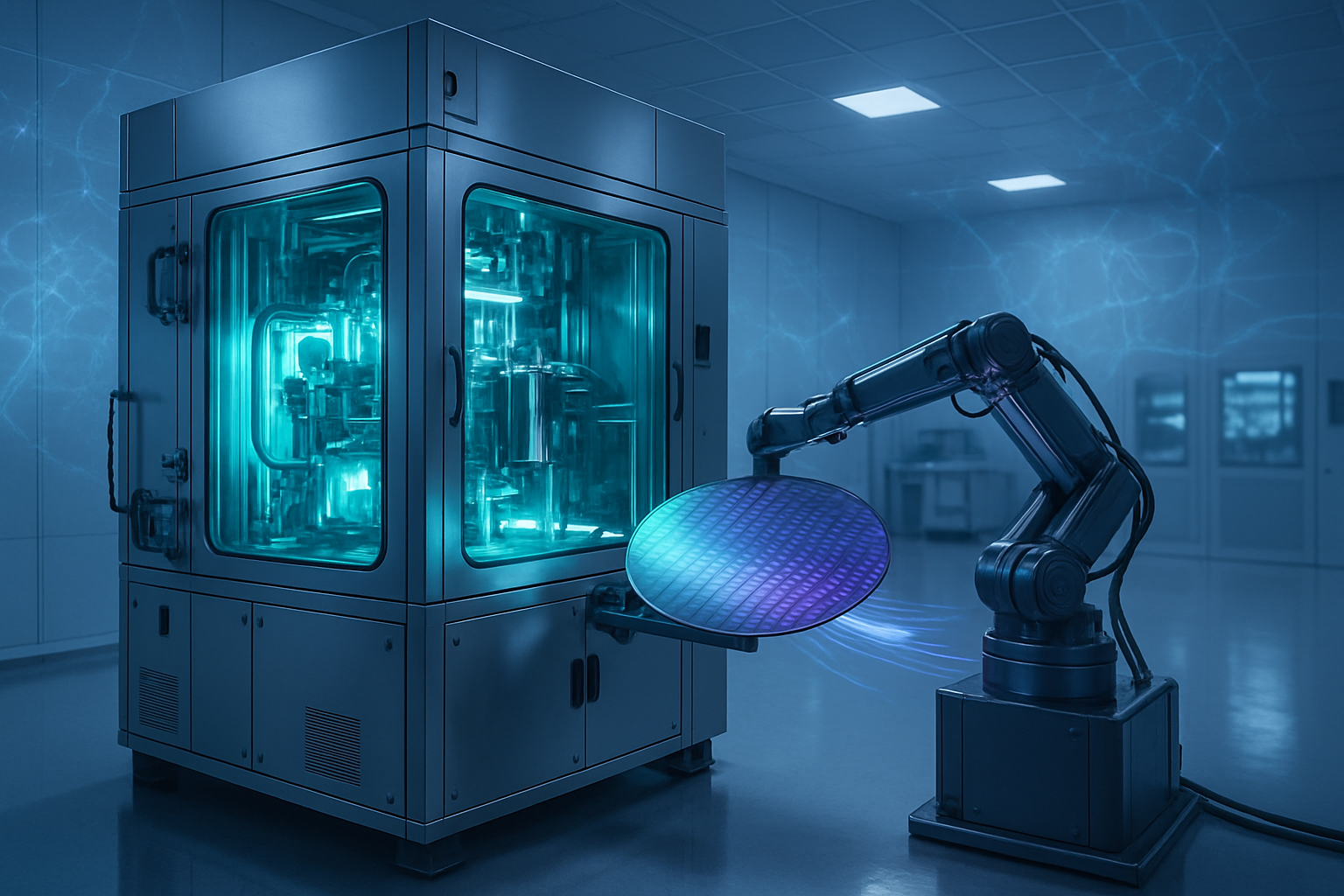
    Veeco Instruments Inc. (NASDAQ: VECO) has unveiled its groundbreaking Lumina+ MOCVD System, a pivotal innovation poised to redefine the landscape of compound semiconductor manufacturing. This advanced Metal-Organic Chemical Vapor Deposition platform is not merely an incremental upgrade; it represents a significant leap forward in enabling the high-volume, cost-effective production of the specialized chips essential for the burgeoning demands of artificial intelligence. By enhancing throughput, uniformity, and wafer size capabilities, the Lumina+ system is set to become a cornerstone in the development of faster, more efficient, and increasingly powerful AI hardware, accelerating the pace of innovation across the entire tech industry.

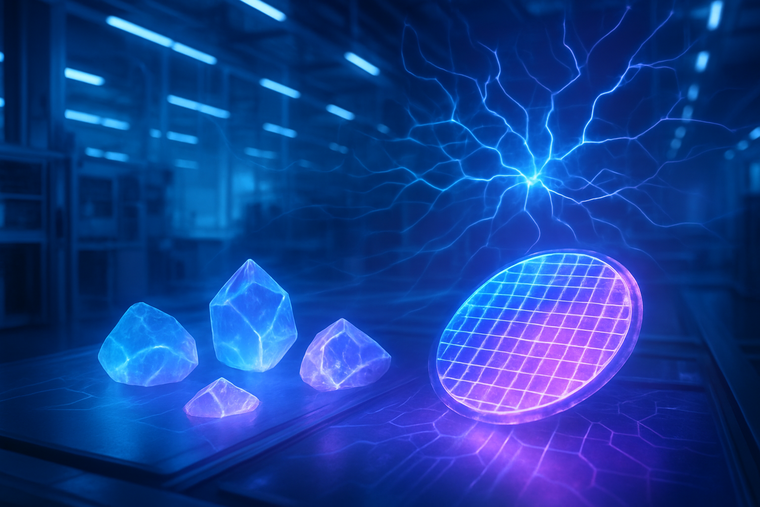
    The immediate significance of the Lumina+ lies in its ability to address critical bottlenecks in the production of compound semiconductors—materials that offer superior electronic and optical properties compared to traditional silicon. As AI models grow in complexity and data processing requirements skyrocket, the need for high-performance components like VCSELs, edge-emitting lasers, and advanced LEDs becomes paramount. Veeco's new system promises to scale the manufacturing of these components, driving down costs and making advanced AI hardware more accessible for a wider range of applications, from autonomous vehicles to advanced data centers and immersive AR/VR experiences.

    Technical Prowess: Unpacking the Lumina+ Advancements

    The Lumina+ MOCVD System distinguishes itself through a suite of technological advancements designed for unparalleled performance and efficiency in compound semiconductor deposition. At its core, the system boasts the industry's largest arsenic phosphide (As/P) batch size, a critical factor for manufacturers aiming to reduce per-wafer costs and significantly boost overall output. This capacity, combined with best-in-class throughput, positions the Lumina+ as a leading solution for high-volume production, directly translating to a lower cost per wafer—a key metric for economic viability in advanced manufacturing.

    A cornerstone of Veeco's (NASDAQ: VECO) MOCVD technology is its proprietary TurboDisc® technology, which the Lumina+ seamlessly integrates and enhances. This proven reactor design is renowned for delivering exceptional thickness and compositional uniformity, low defectivity, and high yield over extended production campaigns. The TurboDisc® system employs a high-speed vertical rotating disk reactor and a sophisticated gas-distribution showerhead, creating optimal boundary layer conditions that minimize particle formation and contamination. This meticulous control is crucial for producing the high-precision epitaxial layers required for cutting-edge optoelectronic devices.

    A significant upgrade from its predecessor, the original Lumina platform which supported up to six-inch wafers, the Lumina+ now enables the deposition of high-quality As/P epitaxial layers on wafers up to eight inches in diameter. This seamless transition to larger wafer sizes without compromising process conditions, film uniformity, or composition is a game-changer for scaling production and achieving greater economies of scale. Furthermore, the system incorporates advanced process control mechanisms, including Veeco's Piezocon® gas concentration sensor, ensuring precise control of metal-organic flux. This level of precision is indispensable for manufacturing complex photonic integrated circuits (PICs) and microLED chips, guaranteeing identical deposition conditions across multiple MOCVD systems and enhancing overall product consistency.

    Initial reactions from the AI research community and industry experts highlight the Lumina+'s potential to accelerate foundational AI research by providing access to more advanced and cost-effective hardware. Compared to previous MOCVD systems, which often struggled with the balance between high throughput and stringent uniformity requirements for larger wafers, the Lumina+ offers a comprehensive solution. Its ability to achieve over 300 runs between chamber cleans also translates into system uptime exceeding 95%, a stark improvement that directly impacts production efficiency and operational costs, setting a new benchmark for MOCVD technology.

    Impact on the AI Ecosystem: Beneficiaries and Competitive Shifts

    The introduction of Veeco's (NASDAQ: VECO) Lumina+ MOCVD System is poised to send ripples throughout the artificial intelligence ecosystem, creating significant advantages for a diverse range of companies, from established tech giants to agile startups. Companies heavily invested in the development and deployment of next-generation AI hardware stand to benefit most directly. This includes firms specializing in optical communications, 3D sensing, LiDAR, augmented and virtual reality (AR/VR), and high-efficiency power electronics—all sectors where compound semiconductors are critical enablers.

    For major AI labs and tech companies like NVIDIA (NASDAQ: NVDA), Google (NASDAQ: GOOGL), Microsoft (NASDAQ: MSFT), and Amazon (NASDAQ: AMZN), which are constantly pushing the boundaries of AI model size and computational demands, the Lumina+ offers a pathway to more powerful and energy-efficient AI accelerators. The system's ability to produce high-quality VCSELs and edge-emitting lasers at scale will directly impact the performance of optical interconnects within data centers and between AI chips, reducing latency and increasing bandwidth—critical for distributed AI training and inference. Furthermore, the enhanced production capabilities for advanced displays (mini/microLEDs) will fuel innovation in human-machine interfaces for AI, particularly in AR/VR applications where visual fidelity and efficiency are paramount.

    The competitive implications are substantial. Manufacturers who adopt the Lumina+ early will gain a strategic advantage in cost-effectively scaling their production of compound semiconductor components. This could lead to a disruption in existing supply chains, as companies capable of producing these specialized chips at lower costs and higher volumes become preferred partners. For instance, Rocket Lab (NASDAQ: RKLB), a global leader in launch services and space systems, has already placed a multi-tool order for the Lumina+ system, leveraging it to double their production capacity for critical components like space-grade solar cells under the Department of Commerce’s CHIPS and Science Act initiatives. This demonstrates the immediate market positioning and strategic advantages conferred by the Lumina+ in enabling domestic production and enhancing national technological resilience.

    Startups focused on novel AI hardware architectures or specialized sensing solutions could also find new opportunities. The lowered cost per wafer and increased production efficiency might make previously unfeasible hardware designs economically viable, fostering a new wave of innovation. The Lumina+ essentially democratizes access to advanced compound semiconductor manufacturing, enabling a broader array of companies to integrate high-performance optoelectronic components into their AI products and services, thereby accelerating the overall pace of AI development and deployment.

    Wider Significance: Reshaping the AI Landscape

    The advent of Veeco's (NASDAQ: VECO) Lumina+ MOCVD System represents more than just a technological upgrade; it signifies a pivotal moment in the broader AI landscape, aligning perfectly with the escalating demand for specialized, high-performance computing. As AI models become increasingly sophisticated and data-intensive, the limitations of traditional silicon-based architectures are becoming apparent. Compound semiconductors, with their inherent advantages in speed, energy efficiency, and optical properties, are emerging as the fundamental building blocks for next-generation AI, and the Lumina+ is the engine driving their mass production.

    This development fits squarely into the overarching trend of hardware-software co-design in AI, where advancements in physical components directly enable breakthroughs in algorithmic capabilities. By making high-quality VCSELs for 3D sensing, LiDAR, and high-speed data communication more accessible and affordable, the Lumina+ will accelerate the development of autonomous systems, robotics, and advanced perception technologies that rely heavily on rapid and accurate environmental understanding. Similarly, its role in producing edge-emitting lasers for advanced optical communications and silicon photonics will underpin the high-bandwidth, low-latency interconnects crucial for hyperscale AI data centers and distributed AI inference networks.

    The impacts extend beyond mere performance gains. The Lumina+ contributes to greater energy efficiency in AI hardware, a growing concern given the massive power consumption of large AI models. Compound semiconductors often operate with less power and generate less heat than silicon, leading to more sustainable and cost-effective AI operations. However, potential concerns include the complexity of MOCVD processes and the need for highly skilled operators, which could pose a challenge for widespread adoption without adequate training and infrastructure. Nonetheless, the system's high uptime and advanced process control aim to mitigate some of these operational complexities.

    Comparing this to previous AI milestones, the Lumina+ can be seen as an enabler akin to the development of advanced GPUs in the early 2010s, which unlocked the deep learning revolution. While not a direct AI algorithm breakthrough, it is a foundational manufacturing innovation that will indirectly fuel countless AI advancements by providing the necessary hardware infrastructure. It underpins the shift towards photonics and advanced materials in computing, moving AI beyond the confines of purely electronic processing and into an era where light plays an increasingly critical role in data handling.

    Future Developments: The Road Ahead for AI Hardware

    Looking ahead, the Veeco (NASDAQ: VECO) Lumina+ MOCVD System is poised to be a catalyst for several near-term and long-term developments in AI hardware. In the near term, we can expect a surge in the availability and affordability of high-performance compound semiconductor components. This will directly translate into more powerful and efficient AI accelerators, improved sensors for autonomous systems, and higher-resolution, more energy-efficient displays for AR/VR applications. Companies currently limited by the cost or scalability of these components will find new avenues for product innovation and market expansion.

    On the horizon, the long-term implications are even more profound. The Lumina+ paves the way for advanced photonic integrated circuits (PICs) to become a standard in AI computing, potentially leading to entirely new architectures where light-based communication and computation minimize energy loss and maximize speed. This could enable true optical AI processors, a significant leap beyond current electronic designs. Furthermore, the ability to produce high-quality mini and microLEDs at scale will accelerate the development of truly immersive and interactive AI experiences, where seamless visual feedback is critical.

    However, several challenges need to be addressed to fully realize the potential of these developments. Continued research into novel compound semiconductor materials and deposition techniques will be crucial to push performance boundaries even further. The integration of these advanced components into complex AI systems will also require sophisticated packaging and interconnect technologies. Additionally, the industry will need to cultivate a skilled workforce capable of operating and maintaining these advanced MOCVD systems and designing with these new materials.

    Experts predict that the Lumina+'s impact will be felt across various sectors, from quantum computing, where precise material control is paramount, to advanced medical imaging and biotechnology, which can leverage high-performance optoelectronic devices. The system's emphasis on scalability and cost-effectiveness suggests a future where advanced AI hardware is not a niche luxury but a widespread commodity, driving innovation across the entire technological spectrum. We can anticipate further optimization of MOCVD processes, potentially leading to even larger wafer sizes and more complex multi-layer structures, continuously pushing the envelope of what's possible in AI hardware.

    Wrap-up: A New Dawn for AI's Foundation

    In summary, Veeco's (NASDAQ: VECO) Lumina+ MOCVD System marks a definitive inflection point in the manufacturing of compound semiconductors, laying a crucial foundation for the next generation of artificial intelligence hardware. The system's unparalleled features—including the largest As/P batch size, best-in-class throughput, lowest cost per wafer, and support for eight-inch wafers—represent significant technological leaps. These advancements, built upon the proven TurboDisc® technology and enhanced with precise process control, directly address the escalating demand for high-performance, energy-efficient components vital for complex AI applications.

    This development's significance in AI history cannot be overstated; it is a critical enabler that will accelerate the transition from silicon-centric AI hardware to more advanced compound semiconductor and photonic-based solutions. By making the production of components like VCSELs, edge-emitting lasers, and advanced LEDs more scalable and cost-effective, the Lumina+ is poised to democratize access to cutting-edge AI capabilities, fostering innovation across startups, tech giants, and specialized hardware developers alike. Its impact will be seen in faster AI models, more intelligent autonomous systems, and more immersive AR/VR experiences.

    The long-term impact of the Lumina+ extends to shaping the very architecture of future computing, moving towards a paradigm where light plays an increasingly central role in processing and communication. While challenges related to material science and integration remain, the trajectory set by Veeco's innovation is clear: a future where AI hardware is not just more powerful, but also more efficient, sustainable, and capable of addressing the most complex challenges facing humanity.

    In the coming weeks and months, industry watchers should keenly observe the adoption rate of the Lumina+ system across the compound semiconductor manufacturing landscape. Key indicators will include new customer announcements, production ramp-ups from early adopters like Rocket Lab (NASDAQ: RKLB), and the subsequent unveiling of AI hardware products leveraging these newly scalable components. The ripple effects of this foundational manufacturing breakthrough will undoubtedly redefine the competitive landscape and accelerate the evolution of AI as we know it.

    This content is intended for informational purposes only and represents analysis of current AI developments.

    TokenRing AI delivers enterprise-grade solutions for multi-agent AI workflow orchestration, AI-powered development tools, and seamless remote collaboration platforms.
    For more information, visit https://www.tokenring.ai/.

  • MOCVD Systems Propel Semiconductor Innovation: Veeco’s Lumina+ Lights Up the Future of Compound Materials

    MOCVD Systems Propel Semiconductor Innovation: Veeco’s Lumina+ Lights Up the Future of Compound Materials

    In a landscape increasingly dominated by the demand for faster, more efficient, and smaller electronic components, the often-unsung hero of advanced manufacturing, Metal Organic Chemical Vapor Deposition (MOCVD) technology, continues its relentless march of innovation. On the cusp of this advancement is Veeco Instruments Inc. (NASDAQ: VECO), whose new Lumina+ MOCVD system, launched this October 2025, is poised to significantly accelerate the production of high-performance compound semiconductors, critical for everything from next-generation AI hardware to advanced displays and 5G networks.

    MOCVD systems are the foundational bedrock upon which many of today's most sophisticated electronic and optoelectronic devices are built. By precisely depositing atomic layers of material, these systems enable the creation of compound semiconductors—materials composed of two or more elements, unlike traditional silicon. These specialized materials offer unparalleled advantages in speed, frequency handling, temperature resilience, and light conversion efficiency, making them indispensable for the future of technology.

    Precision Engineering: Unpacking the Lumina+ Advancement

    MOCVD, also known as Metal-Organic Vapor Phase Epitaxy (MOVPE), is a sophisticated chemical vapor deposition method. It operates by introducing a meticulously controlled gas stream of 'precursors'—molecules like trimethylgallium, trimethylindium, and ammonia—into a reaction chamber. Within this chamber, semiconductor wafers are heated to extreme temperatures, typically between 400°C and 1300°C. This intense heat causes the precursors to decompose, depositing ultra-thin, single-crystal layers onto the wafer surface. The precise control over precursor concentrations allows for the growth of diverse material layers, enabling the fabrication of complex device structures.

    This technology is paramount for manufacturing III-V (e.g., Gallium Nitride (GaN), Gallium Arsenide (GaAs), Indium Phosphide (InP)) and II-VI compound semiconductors. These materials are not just alternatives to silicon; they are enablers of advanced functionalities. Their superior electron mobility, ability to operate at high frequencies and temperatures, and efficient light-to-electricity conversion properties make them essential for a vast array of high-performance applications. These include all forms of Light Emitting Diodes (LEDs), from general lighting to mini and micro-LEDs for advanced displays; various lasers like VCSELs for 3D sensing and LiDAR; power electronics utilizing GaN and Silicon Carbide (SiC) for electric vehicles and 5G infrastructure; high-efficiency solar cells; and high-speed RF devices crucial for modern telecommunications. The ability to deposit films less than one nanometer thick ensures unparalleled material quality and compositional control, directly translating to superior device performance.

    Veeco's Lumina+ MOCVD system marks a significant leap in this critical manufacturing domain. Building on the company's proprietary TurboDisc® technology, the Lumina+ introduces several breakthrough advancements. Notably, it boasts the industry's largest arsenic phosphide (As/P) batch size, which directly translates to reduced manufacturing costs and increased output. This, combined with best-in-class throughput and the lowest cost per wafer, sets a new benchmark for efficiency. The system also delivers industry-leading uniformity and repeatability across large As/P batches, a persistent challenge in high-precision semiconductor manufacturing. A key differentiator is its capability to deposit high-quality As/P epitaxial layers on wafers up to eight inches (200mm) in diameter, a substantial upgrade from previous generations limited to 6-inch wafers. This larger wafer size significantly boosts production capacity, as exemplified by Rocket Lab, a long-time Veeco customer, which plans to double its space-grade solar cell production capacity using the Lumina+ system. The enhanced process efficiency, coupled with Veeco's proven uniform injection and thermal control technology, ensures low defectivity and exceptional yield over long production campaigns.

    Reshaping the Competitive Landscape for Tech Innovators

    The continuous innovation in MOCVD systems, particularly exemplified by Veeco's Lumina+, has profound implications for a wide spectrum of technology companies, from established giants to nimble startups. Companies at the forefront of AI development, including those designing advanced machine learning accelerators and specialized AI hardware, stand to benefit immensely. Compound semiconductors, with their superior electron mobility and power efficiency, are increasingly vital for pushing the boundaries of AI processing power beyond what traditional silicon can offer.

    The competitive landscape is set to intensify, as companies that adopt these cutting-edge MOCVD technologies will gain a significant manufacturing advantage. This enables them to produce more sophisticated, higher-performance, and more energy-efficient devices at a lower cost per unit. For consumer electronics, this means advancements in smartphones, 4K and 8K displays, augmented/virtual reality (AR/VR) devices, and sophisticated 3D sensing and LiDAR applications. In telecommunications, the enhanced capabilities are critical for the rollout and optimization of 5G networks and high-speed data communication infrastructure. The automotive industry will see improvements in electric vehicle performance, autonomous driving systems, and advanced sensor technologies. Furthermore, sectors like aerospace and defense, renewable energy, and data centers will leverage these materials for high-efficiency solar cells, robust RF devices, and advanced power management solutions. Veeco (NASDAQ: VECO) itself stands to benefit directly from the increased demand for its innovative MOCVD platforms, solidifying its market positioning as a key enabler of advanced semiconductor manufacturing.

    Broader Implications: A Catalyst for a New Era of Electronics

    The advancements in MOCVD technology, spearheaded by systems like the Lumina+, are not merely incremental improvements; they represent a fundamental shift in the broader technological landscape. These innovations are critical for transcending the limitations of silicon-based electronics in areas where compound semiconductors offer inherent advantages. This aligns perfectly with the overarching trend towards more specialized hardware for specific computational tasks, particularly in the burgeoning field of AI.

    The impact of these MOCVD breakthroughs will be pervasive. We can expect to see a new generation of devices that are not only faster and more powerful but also significantly more energy-efficient. This has profound implications for environmental sustainability and the operational costs of data centers and other power-intensive applications. While the initial capital investment for MOCVD systems can be substantial, the long-term benefits in terms of device performance, efficiency, and expanded capabilities far outweigh these costs. This evolution can be compared to past milestones such as the advent of advanced lithography, which similarly enabled entire new industries and transformed existing ones. The ability to grow complex, high-quality compound semiconductor layers with unprecedented precision is a foundational advancement that will underpin many of the technological marvels of the coming decades.

    The Road Ahead: Anticipating Future Developments

    Looking to the future, the continuous innovation in MOCVD technology promises a wave of transformative developments. In the near term, we can anticipate the widespread adoption of even more efficient and advanced LED and Micro-LED technologies, leading to brighter, more color-accurate, and incredibly energy-efficient displays across various markets. The ability to produce higher power and frequency RF devices will further enable next-generation wireless communication and high-frequency applications, pushing the boundaries of connectivity. Advanced sensors, crucial for sophisticated 3D sensing, biometric applications, and LiDAR, will see significant enhancements, improving capabilities in automotive safety and consumer interaction.

    Longer term, compound semiconductors grown via MOCVD are poised to play a pivotal role in emerging computing paradigms. They offer a promising pathway to overcome the inherent limitations of traditional silicon in areas like neuromorphic computing, which aims to mimic the human brain's structure, and quantum computing, where high-speed and power efficiency are paramount. Furthermore, advancements in silicon photonics and optical data communication will enhance the integration of photonic devices into consumer electronics and data infrastructure, leading to unprecedented data transfer speeds. Challenges remain, including the need for continued cost reduction, scaling to even larger wafer sizes beyond 8-inch, and the integration of novel material combinations. However, experts predict substantial growth in the MOCVD equipment market, underscoring the increasing demand and the critical role these technologies will play in shaping the future of electronics.

    A New Era of Material Science and Device Performance

    In summary, the continuous innovation in MOCVD systems is a cornerstone of modern semiconductor manufacturing, enabling the creation of high-performance compound semiconductors that are critical for the next wave of technological advancement. Veeco's Lumina+ system, with its groundbreaking capabilities in batch size, throughput, uniformity, and 8-inch wafer processing, stands as a testament to this ongoing evolution. It is not merely an improvement but a catalyst, poised to unlock new levels of performance and efficiency across a multitude of industries.

    This development signifies a crucial step in the journey beyond traditional silicon, highlighting the increasing importance of specialized materials for specialized applications. The ability to precisely engineer materials at the atomic level is fundamental to powering the complex demands of artificial intelligence, advanced communication, and immersive digital experiences. As we move forward, watching for further innovations in MOCVD technology, the adoption rates of larger wafer sizes, and the emergence of novel applications leveraging these advanced materials will be key indicators of the trajectory of the entire tech industry in the coming weeks and months. The future of high-performance electronics is intrinsically linked to the continued sophistication of MOCVD.

    This content is intended for informational purposes only and represents analysis of current AI developments.

    TokenRing AI delivers enterprise-grade solutions for multi-agent AI workflow orchestration, AI-powered development tools, and seamless remote collaboration platforms.
    For more information, visit https://www.tokenring.ai/.

  • Veeco’s Lumina+ MOCVD System Ignites New Era for Compound Semiconductor Production, Fueling Next-Gen AI Hardware

    Veeco’s Lumina+ MOCVD System Ignites New Era for Compound Semiconductor Production, Fueling Next-Gen AI Hardware

    Veeco (NASDAQ: VECO) has today, October 6, 2025, unveiled its groundbreaking Lumina+ MOCVD System, a significant leap forward in the manufacturing of compound semiconductors. This announcement is coupled with a pivotal multi-tool order from Rocket Lab Corporation (NYSE: RKLB), signaling a robust expansion in high-volume production capabilities for critical electronic components. The Lumina+ system is poised to redefine efficiency and scalability in the compound semiconductor market, impacting everything from advanced AI hardware to space-grade solar cells, and laying a crucial foundation for the future of high-performance computing.

    A New Benchmark in Semiconductor Manufacturing

    The Lumina+ MOCVD system represents a culmination of advanced engineering, building upon Veeco's established Lumina platform and proprietary TurboDisc® technology. At its core, the system boasts the industry's largest arsenic phosphide (As/P) batch size, a critical factor for driving down manufacturing costs and increasing output. This innovation translates into best-in-class throughput and the lowest cost per wafer, setting a new benchmark for efficiency in compound semiconductor production. Furthermore, the Lumina+ delivers industry-leading uniformity and repeatability for As/P processes, ensuring consistent quality across large batches – a persistent challenge in high-precision semiconductor manufacturing.

    What truly sets the Lumina+ apart from previous generations and competing technologies is its enhanced process efficiency, which combines proven TurboDisc technology with breakthrough advancements in material deposition. This allows for the deposition of high-quality As/P epitaxial layers on wafers up to eight inches in diameter, a substantial improvement that broadens the scope of applications. Proprietary technology within the system ensures uniform injection and thermal control, vital for achieving excellent thickness and compositional uniformity in the epitaxial layers. Coupled with the Lumina platform's reputation for low defectivity over long campaigns, the Lumina+ promises exceptional yield and flexibility, directly addressing the demands for more robust and reliable semiconductor components. Initial reactions from industry experts highlight the system's potential to significantly accelerate the adoption of compound semiconductors in mainstream applications, particularly where silicon-based solutions fall short in performance or efficiency.

    Competitive Edge for AI and Tech Giants

    The launch of Veeco's Lumina+ MOCVD System and the subsequent multi-tool order from Rocket Lab (NYSE: RKLB) carry profound implications for AI companies, tech giants, and burgeoning startups. Companies heavily reliant on high-performance computing, such as those developing advanced AI models, machine learning accelerators, and specialized AI hardware, stand to benefit immensely. Compound semiconductors, known for their superior electron mobility, optical properties, and power efficiency compared to traditional silicon, are crucial for next-generation AI processors, high-speed optical interconnects, and efficient power management units.

    Tech giants like NVIDIA (NASDAQ: NVDA), Intel (NASDAQ: INTC), and AMD (NASDAQ: AMD), which are deeply invested in AI hardware development, could see accelerated innovation through improved access to these advanced materials. Faster, more efficient chips enabled by Lumina+ technology could lead to breakthroughs in AI training speeds, inference capabilities, and the overall energy efficiency of data centers, addressing a growing concern within the AI community. For startups focusing on niche AI applications requiring ultra-fast data processing or specific optical sensing capabilities (e.g., LiDAR for autonomous vehicles), the increased availability and reduced cost per wafer could lower barriers to entry and accelerate product development. This development could also disrupt existing supply chains, as companies might pivot towards compound semiconductor-based solutions where performance gains outweigh initial transition costs. Veeco's strategic advantage lies in providing the foundational manufacturing technology that unpins these advancements, positioning itself as a critical enabler in the ongoing AI hardware race.

    Wider Implications for the AI Landscape and Beyond

    Veeco's Lumina+ MOCVD System launch fits squarely into the broader trend of seeking increasingly specialized and high-performance materials to push the boundaries of technology, particularly in the context of AI. As AI models grow in complexity and demand more computational power, the limitations of traditional silicon are becoming more apparent. Compound semiconductors offer a pathway to overcome these limitations, providing higher speeds, better power efficiency, and superior optical and RF properties essential for advanced AI applications like neuromorphic computing, quantum computing components, and sophisticated sensor arrays.

    The multi-tool order from Rocket Lab (NYSE: RKLB), specifically for expanding domestic production under the CHIPS and Science Act, underscores a significant geopolitical and economic impact. It highlights a global effort to secure critical semiconductor supply chains and reduce reliance on foreign manufacturing, a lesson learned from recent supply chain disruptions. This move is not just about technological advancement but also about national security and economic resilience. Potential concerns, however, include the initial capital investment required for companies to adopt these new manufacturing processes and the specialized expertise needed to work with compound semiconductors. Nevertheless, this milestone is comparable to previous breakthroughs in semiconductor manufacturing that enabled entirely new classes of electronic devices, setting the stage for a new wave of innovation in AI hardware and beyond.

    The Road Ahead: Future Developments and Challenges

    In the near term, experts predict a rapid integration of Lumina+ manufactured compound semiconductors into high-demand applications such as 5G/6G infrastructure, advanced automotive sensors (LiDAR), and next-generation displays (MicroLEDs). The ability to produce these materials at a lower cost per wafer and with higher uniformity will accelerate their adoption across these sectors. Long-term, the impact on AI could be transformative, enabling more powerful and energy-efficient AI accelerators, specialized processors for edge AI, and advanced photonics for optical computing architectures that could fundamentally change how AI is processed.

    Potential applications on the horizon include highly efficient power electronics for AI data centers, enabling significant reductions in energy consumption, and advanced VCSELs for ultra-fast data communication within and between AI systems. Challenges that need to be addressed include further scaling up production to meet anticipated demand, continued research into new compound semiconductor materials and their integration with existing silicon platforms, and the development of a skilled workforce capable of operating and maintaining these advanced MOCVD systems. Experts predict that the increased availability of high-quality compound semiconductors will unleash a wave of innovation, leading to AI systems that are not only more powerful but also more sustainable and versatile.

    A New Chapter in AI Hardware and Beyond

    Veeco's (NASDAQ: VECO) launch of the Lumina+ MOCVD System marks a pivotal moment in the evolution of semiconductor manufacturing, promising to unlock new frontiers for high-performance electronics, particularly in the rapidly advancing field of artificial intelligence. Key takeaways include the system's unprecedented batch size, superior throughput, and industry-leading uniformity, all contributing to a significantly lower cost per wafer for compound semiconductors. The strategic multi-tool order from Rocket Lab (NYSE: RKLB) further solidifies the immediate impact, ensuring expanded domestic production of critical components.

    This development is not merely an incremental improvement; it represents a foundational shift that will enable the next generation of AI hardware, from more efficient processors to advanced sensors and optical communication systems. Its significance in AI history will be measured by how quickly and effectively these advanced materials are integrated into AI architectures, potentially leading to breakthroughs in computational power and energy efficiency. In the coming weeks and months, the tech world will be watching closely for further adoption announcements, the performance benchmarks of devices utilizing Lumina+ produced materials, and how this new manufacturing capability reshapes the competitive landscape for AI hardware development. This content is intended for informational purposes only and represents analysis of current AI developments.

    TokenRing AI delivers enterprise-grade solutions for multi-agent AI workflow orchestration, AI-powered development tools, and seamless remote collaboration platforms.
    For more information, visit https://www.tokenring.ai/.